
On May 16th, it was announced that Intel had completed the assembly of the industry’s first commercial High Numerical Aperture (High NA) EUV lithography machine. Reports indicate that Intel has secured the entire production capacity of ASML’s High NA EUV lithography machines for this year. In contrast, TSMC has shown less enthusiasm for adopting High NA EUV lithography machines; their latest A16 (1.6nm) process will not use this equipment.
Recently, TSMC’s Senior Vice President of Business Development, Zhang Xiaoqiang, stated that although they are impressed with the capabilities of High NA EUV, the equipment is too expensive (over 300 million euros). Therefore, TSMC will continue using the current conventional EUV equipment for several more years, including for the A16 process.
Zhang pointed out that TSMC’s existing EUV capability can support chip production until the end of 2026 when the A16 process technology will be launched according to the current roadmap.
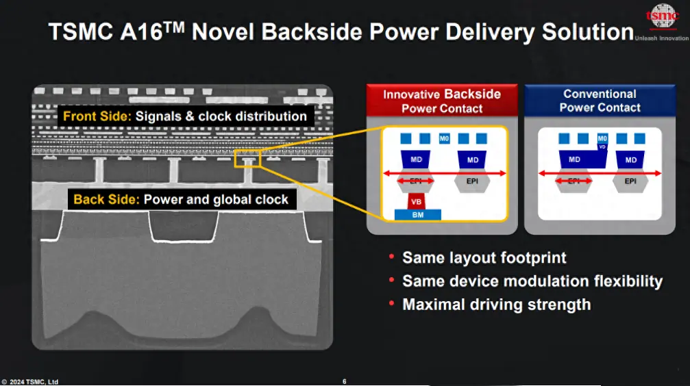
It is reported that A16 will combine TSMC’s Super PowerRail architecture with nanosheet transistors, and mass production is expected in 2026. Compared to the N2P process, A16 will offer an 8-10% speed increase at the same Vdd (operating voltage), a 15-20% reduction in power consumption at the same speed, and a chip density increase of up to 1.10 times to support data center products.
Meanwhile, Intel is actively pursuing the latest High NA EUV lithography machines to achieve a lead over TSMC in process technology. These machines are expected to be used in the mass production of Intel’s 14A process. The Intel 18A process, expected to be commercialized in 2025, will continue to use conventional Low NA EUV lithography machines to achieve the best balance of process technology and cost-effectiveness.
Intel stated that high-NA EUV can reduce the number of masks, improve resolution, and simplify the chip manufacturing process. Masks contain chip designs, and older machines rely on more masks to produce higher-resolution chips.
Related:
- How Megasonic Waves Are Made in Wafer Cleaners?
- Exploring Why Server CPUs Use Hundreds of Powerful Cores
- How ASML Builds Its Billion-Dollar Lithography Machines?

Disclaimer: This article is created by the original author. The content of the article represents their personal opinions. Our reposting is for sharing and discussion purposes only and does not imply our endorsement or agreement. If you have any objections, please contact us through the provided channels.