
In the field of semiconductor manufacturing, interconnect materials function like the “neural network” of electronic devices, playing a crucial role in connecting circuit components, transmitting signals, and supplying power. As chip fabrication technology advances toward the nanoscale, the evolution and upgrading of interconnect materials has become a key driver of semiconductor technology development. This article introduces the development history of semiconductor interconnect materials, compares different interconnect materials, analyzes the reasons why copper replaced aluminum from a theoretical perspective, and discusses future prospects—full of valuable insights!
01
Evolution of Semiconductor Interconnect Materials
In the early days of integrated circuits, limited by technological capabilities, gold was selected as the interconnect material. In the 1950s to early 1960s, gold became the industry’s first choice due to its excellent electrical conductivity (second only to silver), chemical stability, and good compatibility with semiconductor materials. However, its high cost made it unsuitable for large-scale commercial production.
From the 1960s to the mid-1990s, aluminum came to the forefront due to its low cost and ease of processing. Its good etching performance (suitable for both dry and wet etching processes) made it the ideal choice for IC manufacturing at the time and allowed it to dominate the semiconductor industry for over 30 years.
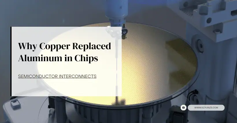
In 1997, IBM introduced advanced copper interconnect technology, marking the beginning of copper gradually replacing aluminum as the core interconnect material in high-performance integrated circuits and ushering in a new era for semiconductor interconnect materials.
02
Performance Comparison of Three Generations of Interconnect Materials
| Material | Conductivity | Chemical stability | Machinability | Cost | Main advantages | Key defect |
|---|---|---|---|---|---|---|
| Gold | Best | High | Better | High | Conductive, strong stability | High cost |
| Aluminum | Better | Normal | Best | Low | Low cost, Easy to process | Electromigration issues |
| Copper | Best | Process control required | Special craftsmanship | Lower | Low resistance, high reliability | Etching difficulties |
03
The Inevitable Replacement of Aluminum by Copper
(1) Performance Bottlenecks Forcing Technological Innovation
As chip fabrication moves toward the nanoscale, the inherent drawbacks of aluminum become increasingly prominent, with electromigration being especially problematic. Aluminum is prone to electromigration due to its physical and chemical properties and operating environment:
✅ Atomic Structure Characteristics
Aluminum atoms have fewer outer electrons and weaker bonding strength, making them more likely to be displaced from their lattice positions under the impact of electron flow. When current passes through an aluminum wire, collisions between electrons and aluminum atoms transfer momentum, causing aluminum atoms to move in the direction of the electron flow.
✅ Fewer Outer Electrons:
Aluminum is element 13, with an electron configuration of 2, 8, 3. The outermost shell has only three electrons, fewer than the stable octet configuration. In the periodic table, moving from left to right in the same period, elements have increasing outer electrons. Aluminum is on the left side of the third period, thus having fewer valence electrons.
✅ Weak Outer Electron Bonding:
Aluminum atoms have three electron shells. As the number of shells increases, the nucleus’s attractive force on the outer electrons weakens due to the shielding effect of inner electrons, reducing the effective nuclear charge felt by outer electrons. This makes the outer electrons more susceptible to external influences, weakening their bond strength.
✅ Larger Atomic Radius:
Within the same period, atomic radius decreases from left to right. Aluminum has a relatively large atomic radius among its period peers, meaning its outer electrons are farther from the nucleus. According to Coulomb’s law, the force between charges is inversely proportional to the square of the distance, so the attraction between nucleus and outer electrons decreases significantly as the distance increases, resulting in weaker bonding.
✅ Crystal Structure:
Aluminum’s face-centered cubic structure provides numerous diffusion pathways for atoms, making it easier for aluminum atoms to migrate within the wire, potentially causing wire breakage or voids.
✅ High Temperature Effects:
Heat generated during IC operation accelerates atomic movement in aluminum, increasing the likelihood of atoms escaping lattice constraints. High temperatures can also alter aluminum’s oxide film structure, reducing its resistance to electromigration.
✅ High Current Density:
As chip integration increases, aluminum wire dimensions shrink, raising current density. Higher current density leads to stronger electron wind forces, exacerbating electromigration.
(2) Technical Advantages of Copper
✅ Low Resistivity:
Copper’s resistivity is only 60% that of aluminum (1.68 μΩ·cm vs. 2.82 μΩ·cm), significantly reducing signal delay and improving chip speed.
✅ High Resistance to Electromigration:
Copper atoms form stronger metallic bonds than aluminum, making them less likely to be displaced from lattice positions under electron impact, effectively suppressing electromigration.
✅ High Activation Energy for Diffusion:
Copper atoms require more energy to diffuse in the lattice, making migration less likely under normal operating temperatures and currents, ensuring stability in copper interconnect structures.
✅ Protective Oxide Film:
Copper forms a dense oxide layer in air that shields it from environmental effects and helps restrict atom migration. Compared to aluminum, copper’s oxide film is more stable and offers better protection against electromigration.
✅ Process Compatibility – Dual Damascene Process:
This process overcomes the difficulty of etching copper by first etching trenches and vias in the insulating layer, then filling them via electroplating, and finally flattening the surface with CMP (Chemical Mechanical Polishing), simplifying the manufacturing process.
04
Technological Breakthroughs and Challenges in Copper Interconnects
The dual damascene process is central to copper interconnects: etching vias and trenches into the insulating layer, then electroplating copper and polishing the surface via CMP. This improves interconnect integrity and reduces defect rates, allowing widespread use of copper in advanced nodes.
However, challenges remain: copper reacts with silicon at the interface, increasing resistance. This must be resolved by introducing barrier layers of materials like titanium or nickel. Additionally, long-term stability in high-temperature environments requires further optimization of process parameters.
05
Future Outlook
Although copper is currently the mainstream material for modern semiconductor interconnects, as Moore’s Law nears its physical limits, the industry is exploring next-generation materials. Silver has even better conductivity, while carbon nanotubes and graphene offer exceptional electrical performance, potentially overcoming current technical barriers and advancing interconnect technology to new heights.
From gold to aluminum to copper, each material upgrade has driven a leap forward in semiconductor technology. This microscopic materials revolution not only reflects humanity’s constant push beyond technological limits but also lays a solid foundation for the continued advancement of information technology in the future.
Related:

Disclaimer:
- This channel does not make any representations or warranties regarding the availability, accuracy, timeliness, effectiveness, or completeness of any information posted. It hereby disclaims any liability or consequences arising from the use of the information.
- This channel is non-commercial and non-profit. The re-posted content does not signify endorsement of its views or responsibility for its authenticity. It does not intend to constitute any other guidance. This channel is not liable for any inaccuracies or errors in the re-posted or published information, directly or indirectly.
- Some data, materials, text, images, etc., used in this channel are sourced from the internet, and all reposts are duly credited to their sources. If you discover any work that infringes on your intellectual property rights or personal legal interests, please contact us, and we will promptly modify or remove it.