
In computer systems, 1MB of storage capacity is substantial and expensive. To understand how large and costly 1MB truly is, the most intuitive method is to calculate the physical area it occupies on a chip.
Let’s do the math using one of today’s most advanced manufacturing processes—TSMC’s 5-nanometer (nm) process node.
According to public industry research, under the 5nm process, a high-density static random-access memory (SRAM) bit cell—which stores one bit of data—has an area of about 0.021 square micrometers (µm²). This is an outcome of extreme technological optimization.
Now, let’s calculate the total area of 1MB of SRAM:
First, unit conversions:
1 Byte = 8 bits
1 Kilobyte (KB) = 1024 Bytes
1 Megabyte (MB) = 1024 KB
So, 1MB contains:
1 × 1024 × 1024 × 8 = 8,388,608 bits
Then, total area of 1MB SRAM:
8,388,608 bits × 0.021 µm²/bit ≈ 176,161 µm²
Let’s convert this to square millimeters (mm²):
176,161 µm² = 0.176 mm²
0.176 mm²—how big is that, really?
Let’s find a reference point—the CPU “brain,” namely the processing core.
Take a high-performance core based on AMD’s Zen 3 architecture as an example. Its area is approximately 3.24 mm².
A simple division gives a surprising result: just 1MB of SRAM takes up about 5.4% of the area of a Zen 3 high-performance core.
And that’s just the storage part of the SRAM. Actual use also includes ECC, BIST, controllers, and other surrounding components, increasing the area further.
And it gets more expensive, too.
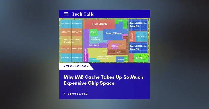
From the CPU die layout in cover image, you can see that even just 512KB (instruction) + 512KB (data) of cache, including control logic, takes up roughly 20% of one CPU core’s area.
Let’s look at real products.
Take the AMD Zen 5 8-core Core Complex Die (CCD) as an example—it packages eight cores and the L3 cache together in a small chip. Using an advanced 4nm process, its total area is about 70.6 mm² and includes 32MB of L3 cache.
The L3 cache takes up nearly 25% of that area—including SRAM, controllers, internal buses, and interconnects.
In other words, in your CPU, the L3 cache region used to hold temporary data occupies more space than 2–3 of the computing cores themselves.
Now you understand why cache is so “precious.”
Even more critically, we’re facing an “SRAM scaling crisis.”
As chip processes advance from 7nm to 5nm to 3nm, logic circuits (i.e., CPU compute units) continue to shrink as expected, but SRAM cells haven’t scaled nearly as well.
For example, in TSMC’s N3E process, the SRAM bit cell area is nearly identical to the earlier N5 process—both around 0.021 µm².
This means that with each new process node, SRAM takes up a larger share of the total chip area.
This creates a major dilemma for chip designers: should they spend precious transistor budget on more powerful compute cores, or on larger caches to feed those cores?
It’s a painful trade-off.
This also explains why the industry is racing to develop radical technologies like 3D V-Cache (vertically stacking cache), because expanding cache area on a flat surface has become increasingly inefficient.
SRAM is so “space-consuming” due to its fundamental design for storing a single bit.
A standard SRAM cell is called a “6T cell” because it requires six transistors to reliably store one bit.
Think of it as a delicate mechanical latch.
At its core are two “cross-coupled inverters” built from four transistors.
It’s like two people, A and B, holding each other’s arms. If A stands up (logic ‘1’), B is forced to squat (logic ‘0’). If A squats, B is pushed to stand up.
They’re always in opposite, stable states.
As long as power is supplied, this state is maintained—hence “static” in SRAM. Unlike DRAM, it doesn’t need to be refreshed constantly.
The remaining two transistors act as “gatekeepers,” known as “access transistors.”
They’re connected to a control line called the “word line.”
When the CPU wants to read or write data, it activates the word line, the “gatekeepers” open the door, and data flows through two “bit lines” into or out of the cell.
This 6T structure is inherently fast and stable.
Since data is “latched” inside, as soon as the door opens, the state is immediately available—resulting in extremely low access latency, usually within a few nanoseconds or even less.
But the cost of this speed and stability is significant area.
The demanding requirements for speed, stability, and size make SRAM a “luxury mansion”: expensive, bulky, but high-performing.
That’s why it’s only used at critical points—inside CPUs as L1, L2, and L3 cache, closest to the computing cores, delivering the fastest data access.
So, if SRAM is so expensive, how do we get tens of gigabytes of main memory in our computers?
The answer is a much more economical solution—Dynamic Random-Access Memory (DRAM).
DRAM has an extremely simple structure: each bit requires only one transistor and one capacitor (1T1C structure).
Compared to SRAM’s six transistors, the difference is dramatic.
This is the key reason why DRAM has much higher density and much lower cost than SRAM.
Here’s a simple analogy for how DRAM works:
Capacitor: like a tiny “bucket” storing electric charge (water). A full bucket = logic ‘1’; an empty one = logic ‘0’.
Transistor: like a “faucet” connected to the bucket, controlling the inflow and outflow of water (data).
But here’s the problem: there’s no such thing as a leak-proof bucket.
At the microscopic scale, the capacitor’s charge leaks very quickly—usually within tens of milliseconds.
Losing data would be catastrophic.
To fix this, engineers invented a refresh mechanism.
There’s a special circuit in the system called the Memory Controller, which acts like a diligent caretaker, periodically checking each “bucket” and refilling (or emptying) them to restore their intended state.
This process is called DRAM refresh.
If you want extreme speed and stability (SRAM), you must pay the price in cost and area.
If you want massive capacity and affordability (DRAM), you must accept slower speeds and the hassle of refreshing.
No technology is perfect.
It’s this imperfection that drives the elegant hierarchy of computer memory systems today: a small amount of expensive SRAM for fast cache, and a large amount of cheap DRAM for main memory.
Back to our original question: is 1MB large?
By now, you should have the answer.
In the world of chips, 1MB is never just a data unit.
It represents 0.176 mm² of precious silicon die area, 8,388,608 precision latch units made from 6T transistors, nanosecond-level access speed, and high manufacturing costs and power consumption.
The “largeness” of 1MB SRAM is physical, economic, and performance-related.
From SRAM’s “luxury villas” to DRAM’s “affordable housing,” and on to DDR “highways” and HBM “vertical cities,” the evolution of memory systems is a journey of pursuing the best balance between speed and density under the constraints of physics and cost.

Disclaimer:
- This channel does not make any representations or warranties regarding the availability, accuracy, timeliness, effectiveness, or completeness of any information posted. It hereby disclaims any liability or consequences arising from the use of the information.
- This channel is non-commercial and non-profit. The re-posted content does not signify endorsement of its views or responsibility for its authenticity. It does not intend to constitute any other guidance. This channel is not liable for any inaccuracies or errors in the re-posted or published information, directly or indirectly.
- Some data, materials, text, images, etc., used in this channel are sourced from the internet, and all reposts are duly credited to their sources. If you discover any work that infringes on your intellectual property rights or personal legal interests, please contact us, and we will promptly modify or remove it.