
In semiconductor processing, SPT usually refers to Stress Proximity Technology. It is a process technology that introduces stress into the semiconductor channel by forming specific structures or depositing specific materials around the gate. The detailed introduction is as follows:
Process Flow:
The core of SPT technology lies in the word “stress.” In semiconductor devices, the mobility of carriers (electrons and holes) directly affects device performance. The SPT process precisely introduces stress into the semiconductor channel by forming specific structures or depositing specific materials around the gate. Its process flow is closely linked and extremely meticulous.
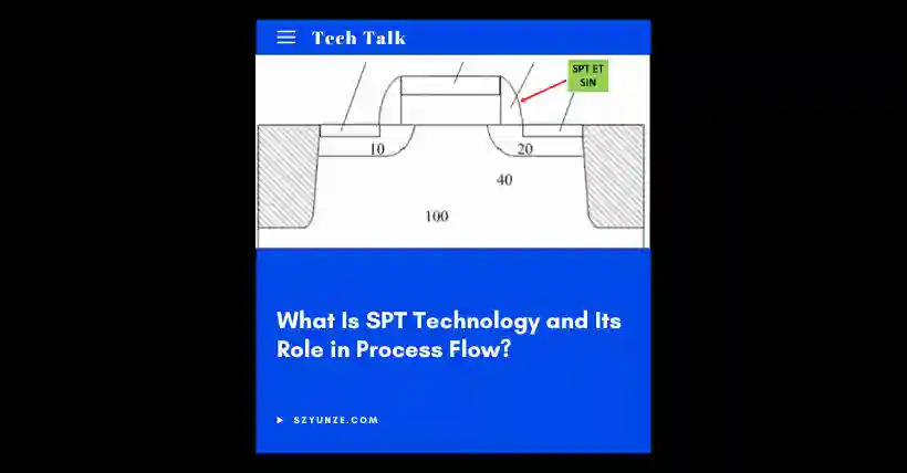
The SPT process begins with the growth of a gate oxide layer and gate on the substrate, which is a crucial foundation for building the basic structure of the device; then, a sidewall oxide layer is formed, and lightly doped drain regions are created through ion implantation and other methods; next, an isolation layer is constructed, and the source/drain regions are formed through windows defined by the isolation layer; partial removal of the sidewalls is carried out through SPT plasma etching; subsequently, high-stress nitride is deposited on the gate, source, and drain regions, bringing the stress film closer to the channel and completing the stress introduction process.
In Stress Proximity Technology (SPT), the etching methods mainly include wet etching and plasma dry etching. In plasma dry etching, the metal silicide of the source and drain regions remains exposed, and this metal silicide plays a decisive role in the resistance of the source/drain regions. Therefore, when using plasma equipment to remove sidewalls, the degree of damage to the metal silicide must be strictly controlled to avoid affecting the performance of the source/drain regions. Sidewall materials are mostly silicon nitride; hence, wet etching usually uses hot phosphoric acid solution as the etchant. Wet etching has significant advantages, with a high selectivity ratio between silicon nitride and metal silicide. Even in cases of substantial over-etching, it can effectively control damage to the metal silicide, thereby ensuring the stability of the source/drain resistance. From an etching characteristics perspective, wet etching is isotropic, differing from the anisotropic nature of plasma dry etching. It can more efficiently achieve sidewall removal. However, wet etching also has drawbacks: during the etching process, particle defects in the chemical container are difficult to control effectively, which may affect the final etching quality.
The function of the SPT process is mainly to improve the electrical performance of MOS devices, specifically in the following aspects:
From a microscopic perspective, it can significantly enhance carrier mobility. Under the effect of the SPT process, a special stress distribution is formed in the channel, with stress gradually increasing from the center to the edge of the channel. This stress distribution breaks the conventional environment for electron or hole movement, creating more efficient migration conditions, and greatly improves the device’s conductivity.
From a macroscopic semiconductor manufacturing perspective, SPT technology also shows significant value. In advanced technologies, the space between adjacent gates becomes increasingly narrow, making gap filling during the formation of the interlayer dielectric (ILD) a major challenge. SPT treatment can effectively improve the margin of the gap-filling process, ensure the smooth progress of the process, and enhance the quality and stability of relevant processes in semiconductor manufacturing.
Moreover, in some processes, by reducing the thickness of the gate sidewalls on both sides of the gate and depositing a stress layer, the distance between the stress layer and the semiconductor substrate and gate can be further reduced. This can significantly enhance the stress effect of the stress layer on the semiconductor substrate and gate, thereby comprehensively improving the performance of semiconductor devices.
As the semiconductor industry advances toward more cutting-edge processes, the importance of SPT technology is becoming increasingly prominent. It is not only a key method for improving the performance of existing semiconductor devices but also an important support for future breakthroughs in chip technology. On the road to achieving higher performance and lower power consumption chips, SPT technology will continue to play a crucial role, working in concert with other semiconductor processes to jointly drive the continuous development of the entire industry.
Related:

Disclaimer:
- This channel does not make any representations or warranties regarding the availability, accuracy, timeliness, effectiveness, or completeness of any information posted. It hereby disclaims any liability or consequences arising from the use of the information.
- This channel is non-commercial and non-profit. The re-posted content does not signify endorsement of its views or responsibility for its authenticity. It does not intend to constitute any other guidance. This channel is not liable for any inaccuracies or errors in the re-posted or published information, directly or indirectly.
- Some data, materials, text, images, etc., used in this channel are sourced from the internet, and all reposts are duly credited to their sources. If you discover any work that infringes on your intellectual property rights or personal legal interests, please contact us, and we will promptly modify or remove it.