
01
Introduction: The Importance of Polysilicon Gates and the Problem of Depletion Effects
In modern integrated circuit manufacturing, the polysilicon gate is a core component of field-effect transistors (FETs), and its performance directly determines the switching characteristics of transistors and the overall functionality of integrated circuits. With excellent electrical performance and high compatibility with existing silicon-based processes, polysilicon gates have long been the preferred material for integrated circuit manufacturing, playing a key role in driving the continuous miniaturization and performance improvement of transistors.
However, as integrated circuit manufacturing advances toward the nanoscale, the depletion effect in polysilicon gates has gradually become a critical bottleneck restricting device performance improvement. This effect not only affects the switching speed and drive capability of transistors but also leads to increased power consumption and reduced reliability, severely hindering further development in the integrated circuit industry.
02
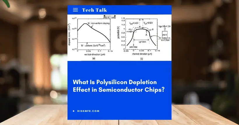
Physical Mechanism of the Depletion Effect
The depletion effect in polysilicon gates originates from changes in charge distribution between the gate and the silicon substrate. When a voltage is applied to the gate, minority carriers are attracted to the dielectric-channel interface, forming an inversion layer. To maintain charge neutrality, carrier accumulation occurs near the interface between the dielectric and the polysilicon, thereby depleting the charge in the adjacent semiconductor. When the semiconductor is fully depleted of charge, the region behaves as an insulator, effectively increasing the gate dielectric’s thickness. Although the depletion layer is extremely thin—equivalent to just a few angstroms of silicon dioxide (about 2–4 Å for NMOS, 3–6 Å for PMOS)—its impact becomes significant in nanoscale processes where gate dielectric thickness is continually reduced. Furthermore, as the gate dielectric becomes thinner, the built-in electric field under the same gate voltage is enhanced, promoting further carrier accumulation and exacerbating the depletion effect.
03
Impact of the Depletion Effect on Device Performance
The depletion effect significantly reduces the electrical performance of devices. Due to the presence of the depletion layer, the gate’s control over the channel weakens, leading to threshold voltage shifts and increased subthreshold swing, which affect the transistor’s switching speed and signal transmission capability. At the same time, the depletion effect increases gate capacitance, prolonging charge/discharge times and further lowering circuit operating frequency. Additionally, the uneven charge distribution caused by the depletion effect increases device leakage current, which not only raises static power consumption but also generates extra heat, affecting the stability and reliability of integrated circuits.
04
Limitations of Traditional Solutions (e.g., Doping Concentration)
Increasing the doping concentration of polysilicon gates was once a common method to mitigate the depletion effect. By increasing the concentration of free carriers, the occurrence of depletion could be reduced. However, as process nodes shrink below 28 nm, this approach faces growing limitations. On the one hand, gate doping concentrations are approaching saturation and are difficult to further increase; on the other hand, high doping concentrations pose serious process challenges. For instance, in PMOS, high-concentration boron doping can easily penetrate the gate dielectric, damaging the device structure and affecting performance and reliability. Currently, NMOS doping concentration must be kept below 10²⁰ cm⁻³, and PMOS doping below 10¹⁹ cm⁻³, making it increasingly difficult to alleviate the depletion effect through doping alone.
05
Introduction of Metal Gates and Their Advantages
Given the limitations of traditional methods, metal gates have been increasingly adopted in sub-28nm nodes, such as in advanced HKMG (High-K Metal Gate) processes. Metals possess an extremely high concentration of free carriers, fundamentally preventing the occurrence of depletion effects. With metal gates, transistor threshold voltage stability is significantly improved, subthreshold swing is reduced, and switching speed and drive capability are greatly enhanced. In addition, metal gates effectively reduce gate resistance and capacitance, minimizing signal transmission delays and increasing circuit operating frequency. The combination of metal gates with high-K dielectrics further optimizes electrical performance and lowers power consumption, providing strong support for the continued advancement of integrated circuits.
06
Conclusion and Future Outlook
The depletion effect in polysilicon gates is a major challenge in the development of nanoscale integrated circuits. The limitations of traditional solutions have made metal gates the mainstream approach. The introduction of metal gates effectively overcomes the impact of depletion effects and greatly improves integrated circuit performance. However, as integrated circuits continue to scale down and demand higher performance, new challenges persist. In the future, it will be necessary to further explore new gate materials and process technologies and to optimize device structure design to meet the increasing demand for high performance and low power consumption, continuously driving innovation and development in the integrated circuit industry.
Related:
- HKMG Technology: Key to Sub-28nm Advanced Node Success
- How Concentration Polarization Affects Wafer Quality?

Disclaimer:
- This channel does not make any representations or warranties regarding the availability, accuracy, timeliness, effectiveness, or completeness of any information posted. It hereby disclaims any liability or consequences arising from the use of the information.
- This channel is non-commercial and non-profit. The re-posted content does not signify endorsement of its views or responsibility for its authenticity. It does not intend to constitute any other guidance. This channel is not liable for any inaccuracies or errors in the re-posted or published information, directly or indirectly.
- Some data, materials, text, images, etc., used in this channel are sourced from the internet, and all reposts are duly credited to their sources. If you discover any work that infringes on your intellectual property rights or personal legal interests, please contact us, and we will promptly modify or remove it.