
01
Preface
The full English name of “EDA” is “Electronic Design Automation,” which is translated into Chinese as 电子设计自动化.
In simple terms, EDA software is the core tool in the field of chip design. It is widely used in integrated circuits (ICs), printed circuit boards (PCBs), and system-level design. Its main function is to improve the efficiency and accuracy of chip design through automation and optimization of the design process.
02
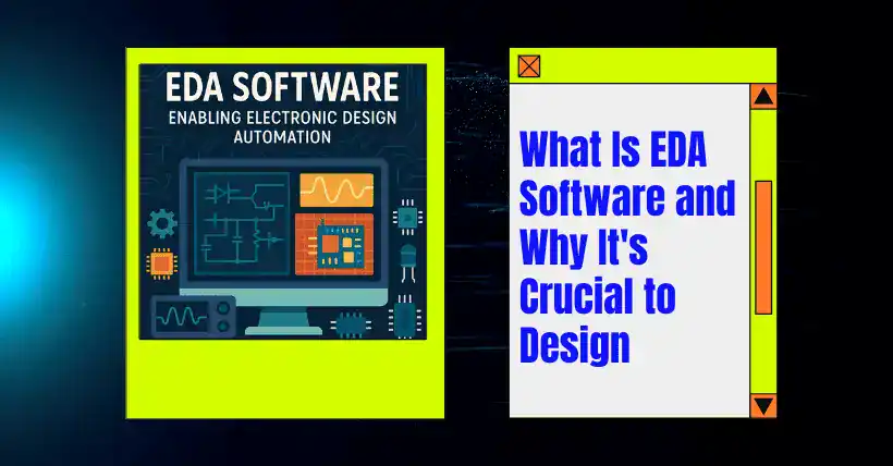
What is EDA Software?
EDA software refers to a category of computer-aided design tools developed specifically for electronic systems and integrated circuit design. Through algorithms, modeling, and simulation technologies, it assists engineers in completing the full workflow from conceptual design to physical implementation. It covers multiple stages of chip design, including logic design, circuit simulation, layout and routing, verification, and manufacturing preparation.
Compared to traditional manual design, EDA software can handle complex design requirements, shorten development cycles, reduce error rates, and optimize chip performance, power consumption, and area, among other aspects.
Modern chips contain billions of transistors and are extremely complex in design, making it almost impossible to complete manually. EDA software automates the process by breaking down complex design tasks into manageable steps and providing visualization, analysis, and optimization tools to help engineers tackle design challenges.
03
Main Functions of EDA Software
EDA software covers the entire chip design process and typically includes the following key modules:
✅ Logic Design and Synthesis
Logic design is the first step in chip design. Engineers use hardware description languages (HDLs, such as Verilog or VHDL) to define the functional behavior of circuits. The synthesis tools in EDA software convert high-level HDL code into gate-level netlists, which describe circuits composed of logic gates and registers. This process requires circuit optimization to meet timing, power, and area requirements.
✅ Circuit Simulation and Verification
Simulation tools are used to verify the correctness of the design, including functional simulation, timing simulation, and power analysis. For example, Cadence’s Incisive Enterprise Simulator can simulate circuit behavior under different conditions. Verification tools (such as Synopsys VCS) use formal verification or dynamic simulation to ensure the design meets specifications and avoid the high costs of late-stage modifications.
✅ Physical Design
Physical design transforms logical netlists into the physical layout of a chip, including placement, routing, and clock tree synthesis. EDA tools (such as Cadence Innovus or Synopsys IC Compiler) optimize the placement and interconnection of transistors using algorithms to meet manufacturing process requirements.
✅ Design Rule Checking and Verification
Design rule checking and layout-versus-schematic (LVS) verification are critical steps in physical design. EDA tools (such as Mentor Graphics Calibre) are used to check whether the layout complies with manufacturing design rules and to ensure consistency between physical layouts and logical designs.
✅ Manufacturing Preparation
After the design is completed, EDA software generates photomask data (in GDSII or OASIS format) used for chip manufacturing. In addition, tools support design for manufacturability (DFM) to optimize designs for higher manufacturing yield.
✅ Power and Thermal Analysis
As power consumption becomes a key factor in chip design, EDA software provides power analysis and optimization tools to help engineers identify and address power issues early in the design process.
04
Classification of EDA Software
According to their functions and application stages, EDA software can be roughly classified into the following categories:
✅ Front-End Design Tools
Front-end tools are mainly used for logic design and functional verification, including HDL editors, synthesis tools, and simulators. For example, Xilinx’s Vivado Design Suite is used for FPGA design, and Synopsys’ Design Compiler is used for ASIC synthesis.
✅ Back-End Design Tools
Back-end tools focus on physical design and manufacturing preparation, including layout and routing, timing analysis, and design rule checking. Cadence Innovus and Synopsys IC Compiler are representative tools in this field.
✅ System-Level Design Tools
System-level design tools are used for the architecture design of complex SoCs or multi-chip systems, such as MathWorks’ MATLAB/Simulink or Cadence’s System Development Suite.
✅ Specialized Tools
Some EDA tools target specific fields, such as analog/mixed-signal design (Cadence Virtuoso), RF circuit design, or memory design.
05
Major EDA Software Vendors
Currently, the global EDA software market is dominated by three major companies:
✅ Synopsys
Synopsys is a leader in the EDA industry, offering a comprehensive suite of tools covering the entire flow from logic synthesis to physical design. Its flagship products include Design Compiler, VCS, IC Compiler, and PrimeTime (timing analysis). Synopsys has also made significant innovations in AI-driven EDA tools (such as DSO.ai).
✅ Cadence Design Systems
Cadence provides full-flow tools from front-end to back-end. Its products include Virtuoso (analog/mixed-signal design), Innovus (physical design), and Incisive (simulation and verification). Cadence is widely used in the fields of 5G, AI, and automotive electronics.
✅ Siemens EDA
Siemens EDA is known for Calibre (design rule checking and verification), and also provides tools such as Tessent (testing) and Veloce (hardware simulation), widely used in chip verification and testing.
In addition, companies like Ansys, Keysight, and Altium have made significant contributions in specific fields such as PCB design or power analysis. Open-source EDA tools (such as OpenROAD and Yosys) have also been gaining traction in recent years, offering low-cost alternatives for small and medium-sized enterprises.
06
Summary
In conclusion, EDA software is the cornerstone of the chip design field, running through every stage of chip design, verification, and manufacturing. From logic synthesis to physical layout, from functional verification to manufacturing preparation, EDA tools greatly enhance the efficiency and quality of chip design through automation and optimization.
Related:
- What Are Chicken Bits in Semiconductor Chip Design?
- A Complete Overview of the Semiconductor Industry Chain
- Improve PCB Cooling Easily with Smart Design Ideas
- Timeline from Design to Finished Photomask Output

Disclaimer: This article is created by the original author. The content of the article represents their personal opinions. Our reposting is only for sharing and discussion purposes and does not imply our endorsement or agreement. If you have any objections, please get in touch with us through the provided channels.