
01
What is Cgd capacitance?
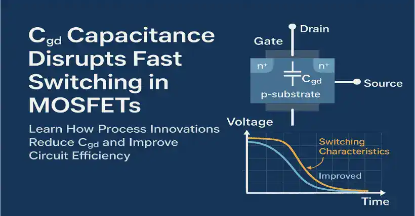
Imagine a MOSFET as a faucet: the gate (G) is the handle, the drain (D) is the spout, and the source (S) is the water inlet. Cgd is the “invisible wire” (capacitance) between the handle and the spout, making the switching action less crisp.
Cgd stands for gate-drain capacitance, which is essentially a natural “invisible connection” between the gate and drain. It’s like two people standing very close—there’s an electrostatic interaction even without direct contact.
02
How does Cgd affect a MOSFET?
When the MOSFET switches, the drain voltage changes rapidly, and this change “sneaks” through Cgd to the gate, disrupting the normal switching signal:
Turn-on process: When trying to turn on the MOSFET, the falling drain voltage pulls down the gate voltage through Cgd—like someone pulling the door from the other side while you’re trying to open it, slowing the action.
Turn-off process: When trying to turn it off, the rising drain voltage pushes up the gate voltage through Cgd—like a gust of wind pushing the door back open as you’re closing it.
Simple rule: The larger the Cgd, the stronger this “interference” and the slower the switching; the smaller the Cgd, the crisper and faster the switching.
03
Why is Cgd important?
Affects efficiency: Slow switching wastes more energy as heat—like a faucet stuck half-open wasting water and leaking.
Can cause malfunction: During fast switching, Cgd may cause unintended conduction—like thinking the faucet is closed, but it starts dripping again.
Impacts circuit frequency: In high-frequency circuits, switching speed directly affects overall performance—like a metronome out of sync ruining the rhythm of a band.
04
Key process optimization techniques
- Spacer process optimization
The spacer process is key to controlling Cgd:
Traditional spacers: Use single SiO₂ material with a relatively high dielectric constant (k≈3.9)
Improved solutions:
- Use low-k dielectric materials (e.g., SiOC, k≈2.7–3.5)
- Employ multilayer composite spacers (SiO₂/SiN stack)
- Optimize spacer width (typically reduced from 50nm to 20nm)
Experimental data shows that using low-k spacer materials can reduce Cgd by 15–20% while maintaining good isolation characteristics.
- Self-aligned process improvements
Modern processes use advanced self-alignment to reduce overlap areas:
- Traditional process: Gate/drain overlap of about 30–50nm
- Advanced process: Ion implantation self-alignment reduces overlap to under 10nm
- Extreme ultraviolet (EUV) lithography enables more precise patterning
- Gate structure innovation
- T-gate structure: Narrows the gate’s bottom width while maintaining top contact area
- Recessed gate: Reduces coupling area between gate and drain
- High-k gate dielectric: Achieves smaller capacitance with the same physical thickness
- Lightly Doped Drain (LDD) optimization
By precisely controlling the LDD region:
- Reduce carrier concentration in the gate-drain overlap region
- Use angled ion implantation to adjust junction depth
- Apply rapid thermal annealing to control dopant distribution

Disclaimer: This article is created by the original author. The content of the article represents their personal opinions. Our reposting is only for sharing and discussion purposes and does not imply our endorsement or agreement. If you have any objections, please get in touch with us through the provided channels.