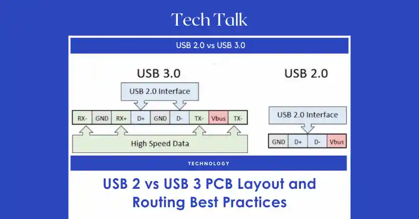
USB is the abbreviation for Universal Serial Bus, a serial bus standard for connecting external devices. It is also a technical specification for input and output interfaces, widely used in information and communication products such as personal computers and mobile devices, and has extended into other related fields such as photographic equipment, digital TVs (set-top boxes), and game consoles.
The USB2.0 interface has a transmission rate of up to 480Mbps, while USB3.0 has a maximum transmission bandwidth of 5Gbps and introduces full-duplex data transmission. The layout and routing of USB have corresponding design requirements.
01
PCB Layout Requirements for USB Interfaces
- The USB interface should be placed near the edge of the board or at a structural positioning point, extending out from the board edge to a certain position (except for straight plug-in types) for easy plugging and unplugging;
- ESD and common-mode inductor components should be placed close to the USB interface, in the order of ESD → common-mode inductor → resistor-capacitor;
- Pay attention to the distance between the ESD and the USB, leaving a certain gap, considering post-soldering conditions;
- When laying out, try to make the differential lines as short as possible to reduce the differential line distance.
02
PCB Routing Requirements for USB Interfaces
- USB should use differential routing, with impedance controlled at 90 ohms and ground shielding, and the total length should preferably not exceed 1800 mils;
- Minimize trace length as much as possible, with priority given to routing high-speed USB differentials (RX, TX differentials). During routing, minimize the number of layer transitions for USB differential lines to better control impedance and avoid signal reflections;
- Vias cause discontinuity in line impedance; at each via layer transition, add a pair of return ground vias for signal return path switching;
- If the positioning pins on both sides of the USB are connected to protective ground, ensure a distance of 2MM from GND during segmentation, and drill more vias in the protective ground area to ensure sufficient connection;
- Due to factors such as pin distribution, vias, and routing space, differential line lengths are prone to mismatch. Once routing lengths are mismatched, timing deviation and common-mode interference may occur, degrading signal quality. Therefore, compensation should be made for unmatched differential pairs to ensure line length matching, usually controlling the length difference within 5 mils. Compensation should follow differential pair length matching standards.
03
PCB Design for Type-C Interface
USB Type-C, also known as USB-C, is just a type of connector and has no relation to the version of USB. The highlights of this interface include a slimmer design, faster transmission speed (up to 10Gbps), and stronger power delivery (up to 100W). The biggest feature of the double-sided plug-in design of Type-C is that it supports USB interface insertion in both directions, mainly targeting thinner and slimmer devices.
PCB Design Requirements for Type-C Interface:
- ESD and common-mode inductor components should be placed close to the Type-C interface, in the order of ESD → common-mode inductor → resistor-capacitor; also pay attention to the distance between ESD and Type-C, leaving a certain gap considering post-soldering;
- The coupling capacitor for TX signal lines should be placed close to the interface, while the coupling capacitor for RX signal lines is provided by the device end;
- Type-C differential routing impedance should be controlled at 90 ohms ±10%. To ensure impedance continuity, there should be a good reference plane with no splits, and the number of signal layer transitions should not exceed two;
- Type-C includes four differential signal groups (RX/TX1-2) and two D+/D− differential signal groups, totaling six pairs of differential lines. Differential signal lines should be adjacent to at least one ground plane, preferably on both sides, with trace length kept short and not exceeding 6 inches;
- Ensure Type-C differential line length matching, with internal length matching error <6 mils, following differential pair length matching standards;
- Ensure the spacing between Type-C differential pairs or between differential pairs and other signals. The recommended internal spacing is greater than or equal to 4 times the Type-C line width. The spacing from other signals should also be at least 4 times the Type-C line width;
- CC1/CC2 are two key pins with multiple functions: detecting connections, distinguishing plug orientation, and identifying DFP/UFP (i.e., host/slave configuration for Vbus). The routing should be thickened.
Note: When the operating speed of the Type-C connector is ≥8Gbps, please follow the connector optimization recommendations in Section 5.6 of Chapter 5 for design processing.
Related:

Disclaimer:
- This channel does not make any representations or warranties regarding the availability, accuracy, timeliness, effectiveness, or completeness of any information posted. It hereby disclaims any liability or consequences arising from the use of the information.
- This channel is non-commercial and non-profit. The re-posted content does not signify endorsement of its views or responsibility for its authenticity. It does not intend to constitute any other guidance. This channel is not liable for any inaccuracies or errors in the re-posted or published information, directly or indirectly.
- Some data, materials, text, images, etc., used in this channel are sourced from the internet, and all reposts are duly credited to their sources. If you discover any work that infringes on your intellectual property rights or personal legal interests, please contact us, and we will promptly modify or remove it.


