
I. Definition of Intrinsic Semiconductors
In simple terms, an intrinsic semiconductor refers to a completely pure, undoped semiconductor with a crystal structure.
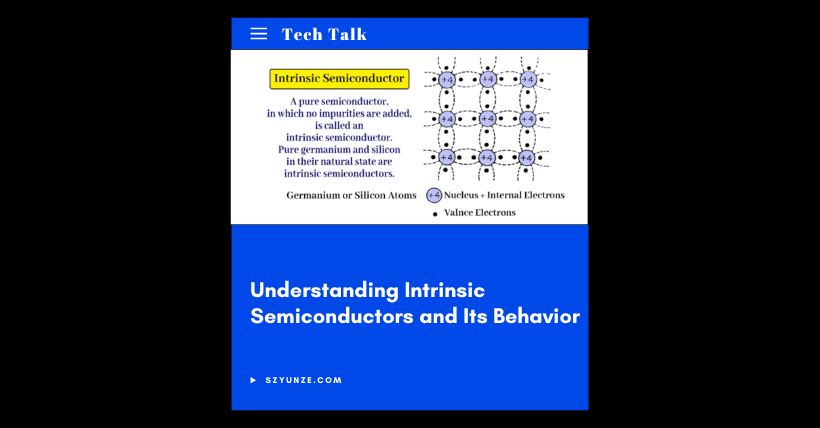
“Pure” means that in the semiconductor material, aside from the atoms forming the basic crystal structure, there are virtually no other impurity atoms. “Crystal structure” refers to atoms being arranged periodically in space according to certain rules, forming a long-range ordered lattice structure.
Common intrinsic semiconductor materials include silicon (Si) and germanium (Ge), both of which belong to Group IV of the periodic table, and their outermost electron shell contains four valence electrons.
Take silicon as an example. A silicon atom connects with four surrounding silicon atoms through covalent bonds, forming a stable crystal structure. In this ideal structure, each silicon atom shares a pair of electrons with adjacent atoms, thereby achieving a stable configuration of eight electrons in its outermost shell. This covalent bond structure is a fundamental feature of intrinsic semiconductors and has a critical impact on their electrical and other properties.
II. Crystal Structure Characteristics of Intrinsic Semiconductors
The crystal structure of intrinsic semiconductors exhibits a high degree of regularity and symmetry. Common intrinsic semiconductor materials include silicon (Si) and germanium (Ge), both of which are in Group IV of the periodic table and have four valence electrons in their outermost shell. Taking silicon as an example, the silicon atoms connect with surrounding silicon atoms through covalent bonds, forming a stable crystal structure.
The electrons in covalent bonds are tightly bound between adjacent atoms. At absolute zero, these electrons have almost no energy to break free from the covalent bonds. At this time, intrinsic semiconductors behave like insulators, with virtually no conductivity.
In this ideal crystal structure, each silicon atom shares a pair of electrons with adjacent atoms, thus fulfilling the stable octet configuration (for some atoms like hydrogen, it is two electrons). This covalent bond structure is the basic structural characteristic of intrinsic semiconductors and plays a vital role in determining their electrical and other properties.
However, when the temperature rises or under external influences such as light, the situation changes. An increase in temperature intensifies the thermal vibrations of atoms, and some electrons may gain enough energy to overcome the bond constraints and become free electrons that can move freely within the crystal. At the same time, a vacancy is left where the electron used to be—this is called a hole.
III. Charge Carriers in Intrinsic Semiconductors
✅ Free Electrons
Free electrons are an important type of charge carrier in intrinsic semiconductors. When electrons gain enough energy to escape the covalent bonds, they become free electrons. These electrons are no longer confined to the vicinity of a specific atom and can move freely throughout the crystal structure.
Free electrons carry a negative charge. Under the influence of an external electric field, they move in the direction opposite to the field, thus forming an electric current. The number of free electrons generated is closely related to temperature: the higher the temperature, the more electrons can overcome the bond constraints, resulting in a higher concentration of free electrons.
✅ Holes
Holes are another unique type of charge carrier in intrinsic semiconductors. When an electron breaks free from a covalent bond and becomes a free electron, it leaves behind a hole at its original position. Although a hole is not a real particle, it behaves like a positively charged particle.
In the crystal, electrons from adjacent covalent bonds can easily move into the hole. After filling the hole, a new hole forms at the original position of the moving electron. This process gives the appearance that the hole is moving through the crystal.
The movement direction of holes is opposite to that of electrons. Under an external electric field, holes move in the direction of the field and also contribute to electrical current. Essentially, hole conduction occurs through successive electron transitions between covalent bonds, but for easier understanding and analysis, holes are typically treated as positively charged carriers.
IV. Electrical Properties of Intrinsic Semiconductors
✅ Electrical Conductivity
The electrical conductivity of intrinsic semiconductors is a key physical quantity measuring their ability to conduct electricity. Conductivity depends on the concentration of free electrons and holes and their mobility. Mobility reflects how easily carriers move under an electric field.
Because intrinsic semiconductors have relatively low carrier concentrations, and their mobility is limited by the crystal structure and other factors, their conductivity is generally low—falling between conductors and insulators. However, it is precisely this unique conductivity that allows intrinsic semiconductors to exhibit rich and useful electrical characteristics after proper doping and treatment, making them the foundation of various semiconductor devices.
✅ Temperature Characteristics
Temperature significantly affects the electrical performance of intrinsic semiconductors. Generally, as the temperature increases, the generation rate of electron-hole pairs increases, carrier concentration rises, and conductivity improves. This close relationship between temperature and conductivity makes intrinsic semiconductors highly sensitive to temperature.
In practical applications, this characteristic can be used to make temperature-sensitive resistors and other sensors. However, it also presents challenges. For instance, in semiconductor devices requiring high temperature stability, special measures must be taken to compensate for temperature effects to ensure stable and reliable operation.
V. Conclusion
In summary, intrinsic semiconductors are very important foundational materials. They not only form one of the cornerstones of the modern microelectronics industry but also provide an ideal experimental platform for in-depth research into semiconductor physics. Although their direct practical applications are limited (they are rarely used in their pure form and are mostly doped for use), understanding and mastering intrinsic semiconductors enables better design and development of high-performance semiconductor devices tailored to various needs.
In future technological development, with the advancement of new materials science and the application of nanotechnology, intrinsic semiconductors are expected to continue playing an important role and to expand into new application areas.

Disclaimer:
- This channel does not make any representations or warranties regarding the availability, accuracy, timeliness, effectiveness, or completeness of any information posted. It hereby disclaims any liability or consequences arising from the use of the information.
- This channel is non-commercial and non-profit. The re-posted content does not signify endorsement of its views or responsibility for its authenticity. It does not intend to constitute any other guidance. This channel is not liable for any inaccuracies or errors in the re-posted or published information, directly or indirectly.
- Some data, materials, text, images, etc., used in this channel are sourced from the internet, and all reposts are duly credited to their sources. If you discover any work that infringes on your intellectual property rights or personal legal interests, please contact us, and we will promptly modify or remove it.