
01
Introduction
Frankly speaking, for ordinary digital technology enthusiasts, understanding the FinFET process can be somewhat challenging because it involves a large amount of related fundamental knowledge and terminology. Only after understanding this foundational knowledge and background can one delve deeper into the subject.
02
Basic Knowledge
Although chips appear advanced, their essence is still based on transistors, which consist of the source (Source), drain (Drain), and gate (Gate). When we refer to XX nanometers, we are talking about the gate’s channel length, which is an important indicator for evaluating the advancement of chip manufacturing technology. The shorter the gate length, the more advanced it is.
However, due to various factors, the gate length cannot be infinitely reduced. When the gate length shrinks to a certain extent, short-channel effects arise, leading to issues like leakage, increased power consumption, and heat generation. Therefore, while pursuing a smaller gate length, comprehensive consideration and optimization of the chip’s performance, power consumption, and stability are also necessary.
03
Birth Background
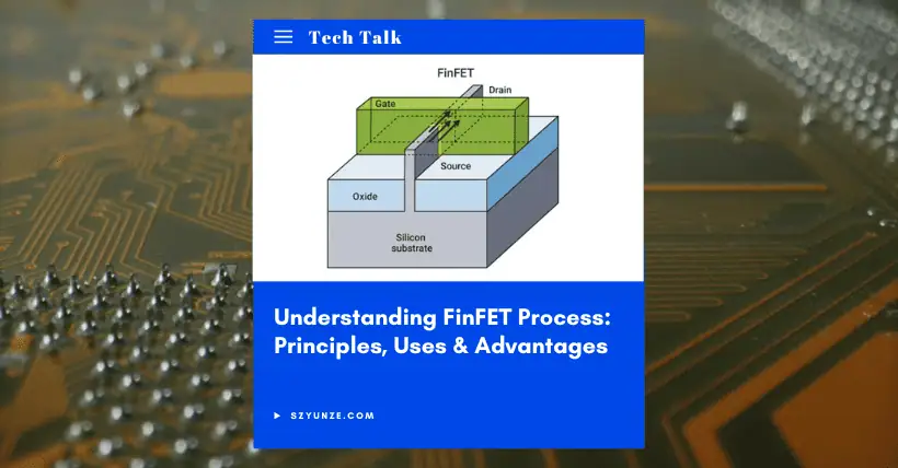
In the earlier years, transistors were flat (see the diagram below). The limit of this design was 22 nanometers. To further improve chip fabrication, it was necessary to make significant reforms and innovations in the existing transistor design concepts. It was in this context that FinFET was born.
The full English name of FinFET is Fin-Field-Effect Transistor, and its Chinese name is 鳍式场效应晶体管 (Fin-style Field-Effect Transistor). Unlike the traditional flat design, the channel of a FinFET transistor is no longer flat, but is vertical to the substrate, resembling a fish fin. This is the origin of its name.
This unique fin-like structure allows the gate to surround the channel from three directions, significantly enhancing the gate’s control over the channel.
04
Operating Principle of FinFET Technology
The operating principle is based on the field-effect principle. When a voltage is applied to the gate, an electric field is formed between the gate and the channel. If the gate voltage is positive (for N-type FinFET), this electric field attracts electrons to accumulate on the surface of the channel, forming a conductive inversion layer that connects the source and drain. At this point, the transistor is turned on, and current can flow from the source to the drain.
On the other hand, when the gate voltage is zero or negative, the carriers in the channel are depleted, the conductive channel disappears, and the transistor is turned off, preventing current from flowing.
Since the gate of a FinFET surrounds the channel from three directions, as opposed to the one-directional gate control of traditional flat transistors, it can more effectively control the carrier concentration and flow in the channel, reducing the impact of short-channel effects.
05
Advantages of FinFET Technology
✅ Improved Performance
The three-dimensional structure of FinFET allows the gate to control the channel from three directions, leading to more precise control over the carriers. This allows the transistor to pass a larger current in the on-state, thereby increasing the chip’s computation speed and processing capacity.
✅ Reduced Power Consumption
FinFET can better control the carriers in the channel, and in the transistor’s off-state, leakage current is significantly reduced. Due to its excellent switching characteristics, FinFET also has lower energy loss during signal switching, helping to reduce the chip’s dynamic power consumption.
06
Development History of FinFET Technology
The concept of FinFET was first proposed by Professor Hu Zhengming of the University of California, Berkeley, in 1990. After years of research and technological accumulation, in 2011, Intel became the first company to introduce FinFET technology into production, applying it to the 22-nanometer process for chip manufacturing.
This move marked the transition of FinFET technology from the laboratory to actual production, ushering in a new era of semiconductor manufacturing technology. Following this, semiconductor manufacturers like Samsung and TSMC also followed suit, continuously advancing and refining the FinFET process.
From the initial 22-nanometer process to today’s 7-nanometer, 5-nanometer, and even more advanced processes, FinFET technology has played a crucial role in continually shrinking transistor sizes and improving chip performance.
07
Conclusion and Outlook
Objectively speaking, FinFET represents a major breakthrough in advancing chip manufacturing processes, but it is not a panacea. At around 3 nanometers, FinFET encounters significant challenges, and several major industry players have adopted different approaches.
TSMC has adopted the FINFLEX process, which is an improved and upgraded version of FinFET. Samsung has adopted the GAAFET (Gate-All-Around Field-Effect Transistor) process, and Intel’s 2-nanometer process, referred to as 20A, will use RibbonFET (Fully-Gated Transistor) and backside power supply technology (see the diagram below). Which approach will be the best is still unknown.
Related:
- What Is Polysilicon Depletion Effect in Semiconductor Chips?
- FET (Field Effect Transistor): Principle & Applications
- Understanding MOSFET: Design, Function and Uses
- HKMG Technology: Key to Sub-28nm Advanced Node Success

Disclaimer:
- This channel does not make any representations or warranties regarding the availability, accuracy, timeliness, effectiveness, or completeness of any information posted. It hereby disclaims any liability or consequences arising from the use of the information.
- This channel is non-commercial and non-profit. The re-posted content does not signify endorsement of its views or responsibility for its authenticity. It does not intend to constitute any other guidance. This channel is not liable for any inaccuracies or errors in the re-posted or published information, directly or indirectly.
- Some data, materials, text, images, etc., used in this channel are sourced from the internet, and all reposts are duly credited to their sources. If you discover any work that infringes on your intellectual property rights or personal legal interests, please contact us, and we will promptly modify or remove it.