
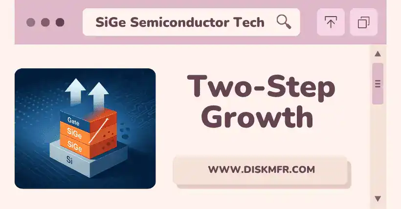
In the SiGe semiconductor process, the two-step growth of a low-doped Ge layer followed by a high-doped Ge layer is mainly based on various process optimization requirements:
01
Mitigating Lattice Mismatch Stress
Lattice constant difference: Ge has a lattice constant (~5.66 Å) about 4% larger than that of Si (~5.43 Å). Directly growing a highly doped Ge layer on a Si substrate results in significant lattice mismatch stress, leading to defects such as dislocations. The first low-doped Ge layer serves as a buffer, with lower doping concentration and gradually varying Ge content (e.g., from Si to SiGe), to gradually release lattice stress and provide a stable foundation for subsequent high-doped layer growth. For example, in the PMOS source/drain region, a low-Ge-content SiGe buffer layer is first grown, followed by a high-Ge-content SiGe epitaxial layer, effectively suppressing strain relaxation and enhancing channel compressive stress.
Graded buffer layer: Growing a low-doped Ge layer (such as a low-Ge-content SiGe layer) first forms a graded lattice transition layer, gradually adapting to the Si substrate’s lattice constant, reducing interfacial defects, and improving the crystal quality of the subsequent high-Ge-concentration layer.
02
Optimizing Electrical Performance
Carrier mobility: A low-doped Ge layer reduces impurity scattering, maintaining high carrier mobility, which is critical for the base performance of high-frequency devices such as HBTs.
Subsequent high doping: Growing a highly doped Ge layer on top of the low-doped layer enables low-resistance contacts (e.g., the base contact of HBTs), while avoiding defects or impurity diffusion caused by premature heavy doping.
03
Strain Engineering Control
Strain modulation: In PMOS devices, the compressive stress introduced by the highly doped SiGe source/drain regions can significantly enhance hole mobility. The stepwise growth allows precise control of stress distribution by adjusting Ge content and doping concentration—for example, forming a “diamond-shaped” SiGe structure near the channel to enhance localized stress. Similarly, in NMOS devices, stepwise epitaxy of SiC or C-doped Si layers can introduce tensile stress to improve electron mobility.
04
Interface Quality and Reliability
Reducing interface defects: The low-doped Ge layer acts as a buffer to smooth the interface, reduce interface state density between highly doped Ge and the Si substrate, and improve device reliability and noise characteristics.
Suppressing diffusion: If a highly doped Ge layer is in direct contact with the Si substrate, dopants (such as boron) may diffuse into the substrate during high-temperature processing. Two-step growth can isolate this effect.
05
Process Flexibility
Independent optimization: The two-step growth allows separate optimization of the crystal quality of the low-doped layer and the electrical properties of the high-doped layer (by adjusting Ge content, doping concentration, and thickness).
Typical Application Example: SiGe Heterojunction Bipolar Transistor (HBT)
Base structure: A low-doped SiGe layer serves as the intrinsic base (for high mobility), and a highly doped SiGe layer serves as the extrinsic base (for low contact resistance). The combination achieves high frequency and high current gain.
06
Conclusion
The two-step growth method, through graded strain control, defect management, and electrical performance optimization, balances material quality with device requirements. It is a key approach in the SiGe process to enhance device performance and reliability.
Related:
- What Is SPT Technology and Its Role in Process Flow?
- Who Holds the Riskiest Jobs in Wafer Fabrication?

Disclaimer:
- This channel does not make any representations or warranties regarding the availability, accuracy, timeliness, effectiveness, or completeness of any information posted. It hereby disclaims any liability or consequences arising from the use of the information.
- This channel is non-commercial and non-profit. The re-posted content does not signify endorsement of its views or responsibility for its authenticity. It does not intend to constitute any other guidance. This channel is not liable for any inaccuracies or errors in the re-posted or published information, directly or indirectly.
- Some data, materials, text, images, etc., used in this channel are sourced from the internet, and all reposts are duly credited to their sources. If you discover any work that infringes on your intellectual property rights or personal legal interests, please contact us, and we will promptly modify or remove it.