
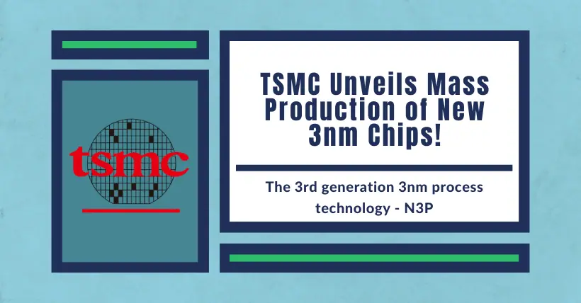
TSMC, the world’s leading semiconductor manufacturer, recently announced the mass production of its third-generation 3nm process technology, N3P, starting in the second half of this year. This news marks another significant breakthrough for TSMC in the field of semiconductor process technology.
It is reported that TSMC successfully initiated chip production using the second-generation 3nm process technology, N3E, in the fourth quarter of 2023, achieving the expected milestone. As an upgrade to N3E, N3P demonstrates significant progress in optical shrinkage and performance enhancement. After the necessary qualification certification, N3P has shown production performance close to N3E and is expected to enter the high-volume manufacturing (HVM) stage in the second half of this year.
The key feature of the N3P process technology is its simplification compared to N3E. By optimizing the production process, N3P removes some layers requiring EUV lithography and completely avoids the use of EUV double patterning, thereby reducing production costs, widening the process window, and increasing yield. While simplifying, N3P also achieves a 4% performance improvement or approximately 9% reduction in power consumption at the same clock speed and increases transistor density for chip designs by 4%.
TSMC stated that N3P maintains compatibility with N3E’s IP modules, design tools, and methods, providing developers with a seamless transition option. Due to the significant advantages of N3P in performance and cost, it is expected that many TSMC customers, including Apple and AMD, will quickly adopt this new technology.
During the mass production preparation process of N3P, TSMC has made significant progress. Currently, N3P has passed the necessary qualification certification and has gained recognition from product customers. TSMC expects that with the mass production of N3P, most new chip designs originally planned for N3E will switch to N3P to fully utilize its higher performance and cost-effectiveness.
Although the launch date of chips based on N3P has not been determined, it is expected that major manufacturers such as Apple will adopt this advanced technology in their 2025 processor lineup. By then, we can expect to see SoC chips incorporating N3P process technology in devices such as smartphones, personal computers, and tablets, offering more powerful performance and more efficient energy consumption.
TSMC’s introduction of the N3P process technology not only demonstrates its leading position in the semiconductor process field but also brings new development opportunities to the entire semiconductor industry. With the mass production and widespread application of N3P, we have reason to expect a brighter future for the semiconductor industry.
Related:
- Samsung DRAM Redesign Aims for Higher Yields by 2025 Q2
- 2025 Semiconductor Outlook: Cutbacks or Growth Ahead?
- SSD Price Cuts Sep. 2024: The Return of Market Pressure
- TSMC Shatters Records: March 2024 Revenue Soars by 34%
- Positive Cycle for NAND Chips Starts June 2024

Disclaimer: This article is created by the original author. The content of the article represents their personal opinions. Our reposting is for sharing and discussion purposes only and does not imply our endorsement or agreement. If you have any objections, please contact us through the provided channels.