
1. Introduction
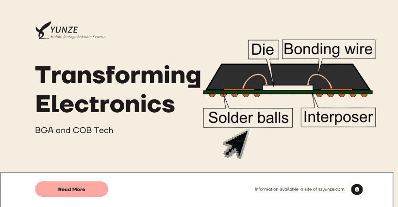
Ball Grid Array (BGA) packaging technology represents a significant advancement in modern integrated circuit packaging. Its uniqueness lies in the presence of a certain number of spherical solder points on the bottom of the chip, which are used to connect to corresponding pads on the motherboard. This design offers higher pin density and more stable connectivity compared to traditional packaging.
2. The Birth of BGA
The history of BGA packaging technology can be traced back to the late 1980s when the complexity and performance requirements of electronic devices were increasing. Traditional packaging technologies, including Dual In-line Package (DIP) and Quad Flat Package (QFP), couldn’t meet these demands, leading to the exploration of new packaging methods.
3. The Brain Behind BGA
The innovation of BGA packaging technology came from engineer Jeffery Harney at IBM in the 1990s. Unlike previous methods, BGA packaging moved the solder pads from the chip’s periphery to the bottom and replaced traditional flat solder points with spherical ones. This structure not only increased pin density but also improved heat dissipation and signal transmission quality.
4. BGA’s Impact
The introduction of BGA packaging opened up new possibilities for the development of integrated circuits. Its high pin density, excellent heat dissipation, and stable signal transmission performance made it widely used in areas such as computers, communication devices, and consumer electronics. As technology advances, BGA packaging continues to evolve, giving rise to new forms like Micro Ball Grid Array (µBGA) and Chip-Scale Ball Grid Array (CSP-BGA) to meet changing market demands.
5. The Evolution Continues
The development of packaging technology is an evolving process, and as technology and market demands change, some packaging methods may be gradually replaced by newer ones. However, BGA (Ball Grid Array) packaging technology remains widely used and an effective and reliable choice in many scenarios.
6. The Advantages of BGA
Despite the emergence of new packaging technologies, BGA packaging still offers unique advantages, especially in high-density integration, compact design, and efficient heat dissipation. Therefore, in some application fields, BGA packaging technology is likely to continue to be adopted.
7. Chip-On-Board (COB) Packaging Technology: A Journey Through Time
① Introduction to COB
Chip-on-board (COB) packaging technology is a method that directly connects bare semiconductor chips (without external packaging) to printed circuit boards (PCBs). The history of this packaging technology can be traced back to the early days of electronic manufacturing, particularly in the early and mid-20th century when it found extensive use in wireless and electronic devices.
② The Early Days
In the early days of electronic manufacturing, packaging integrated circuit chips was often an expensive and complex process. To simplify the manufacturing process and reduce costs, researchers began exploring methods to directly connect chips to PCBs. This direct connection not only reduced the materials required for packaging but also improved the reliability and stability of circuits.
③ Rise of COB
In the 1960s and 1970s, as integrated circuit technology advanced, COB packaging technology became widely adopted. During this period, electronic devices, especially computers and communication equipment, demanded compactness and high performance. COB packaging technology was well-suited for these requirements as it allowed for higher integration and smaller packaging volume.
④ The Evolution
COB packaging technology does not have a specific inventor or invention event but rather evolved and matured gradually with the development of electronic manufacturing technology. The earliest COB packaging processes involved connecting the bare chips’ metal wires to the conductive paths on the PCB. This connection method typically used micro-scale wires and required highly precise operations.
⑤ Modern COB
As manufacturing technology progressed, COB packaging processes were improved and optimized. Modern COB packaging often uses Micro-Electrode Arrays and adhesives to precisely connect chips to PCBs. This technology can achieve high-density and high-reliability packaging and is suitable for various applications, including sensors, medical devices, and consumer electronics.
8. In Conclusion
In summary, the development of COB packaging technology is an evolutionary process that provides crucial support for the miniaturization and high performance of modern electronic devices. However, with the continuous advancement of technology, more advanced and efficient packaging technologies may emerge in the future, replacing the current ones. This replacement is typically influenced by factors such as cost, performance, and reliability.
9. Frequently Asked Questions
1. What are the key advantages of BGA packaging technology?
BGA packaging technology offers higher pin density, improved heat dissipation, and stable signal transmission, making it a popular choice for integrated circuit packaging.
2. How did BGA packaging technology evolve over the years?
BGA packaging technology has evolved to include variations like Micro Ball Grid Array (µBGA) and Chip-Scale Ball Grid Array (CSP-BGA) to meet changing market demands.
3. What are the primary applications of COB packaging technology?
COB packaging is commonly used in applications such as sensors, medical devices, and consumer electronics due to its high-density and high-reliability packaging.
4. Are there any disadvantages to BGA packaging?
While BGA packaging has many advantages, it can be challenging to repair or replace components, making it less suitable for certain scenarios.
5. How does COB packaging technology contribute to the miniaturization of electronic devices?
COB packaging directly connects chips to PCBs, reducing the need for external packaging and allowing for smaller, more compact electronic devices.

Related: