
Tag Archives: PCB Layout and Routing
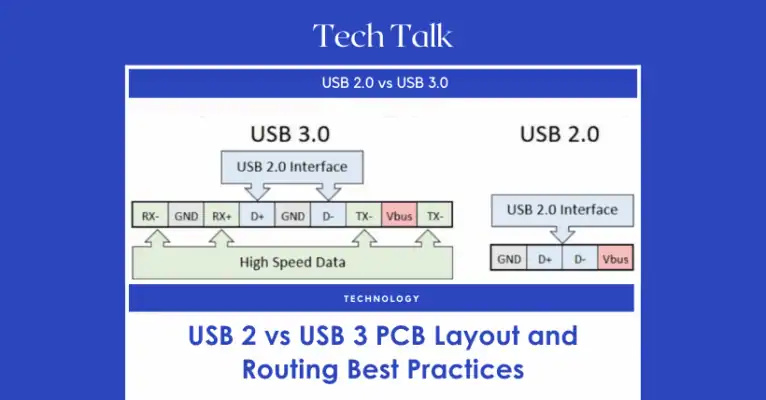
USB 2 vs USB 3 PCB Layout and Routing Best Practices
Master PCB layout and routing for USB 2.0 and 3.0 to boost signal quality, performance, [...]
30
May
May
Master PCB layout and routing for USB 2.0 and 3.0 to boost signal quality, performance, [...]