
NOR Flash and NAND Flash #
NOR Flash and NAND Flash are currently the two main non-volatile flash memory technologies in the market. Intel first developed NOR Flash technology in 1988, completely altering the dominance previously held by EPROM (Electrically Programmable Read-Only Memory) and EEPROM (Electrically Erasable Programmable Read-Only Memory). Subsequently, in 1989, Toshiba introduced the NAND Flash architecture, emphasizing cost reduction per bit, higher performance, and ease of upgrading through interfaces, similar to a disk drive. NOR Flash features execute in place (XIP) within the chip, allowing applications to run directly in the Flash memory without the need to load the code into system RAM. NOR exhibits high transfer efficiency and is cost-effective for small capacities in the range of 1 to 4MB. However, its slow write and erase speeds significantly impact its performance. NAND’s structure offers extremely high cell density, enabling high storage density, with fast write and erase speeds. The challenge with using NAND lies in Flash management and the need for specialized system interfaces. Typically, NOR read speeds are slightly faster than NAND, while NAND’s write speed is considerably faster than NOR. These factors should be considered in the design process.
What is NAND Flash? #
NAND flash memory is a superior storage device compared to traditional hard disk drives. It employs non-volatile storage technology, which means it can retain data even after a power loss.
NAND flash memory consists of multiple storage units organized in bits. These bits are manipulated by electric charges to open or close, and how these switch units are organized to store data on an SSD determines the naming of NAND flash memory types. For example, Single-Level Cell (SLC) flash memory contains one bit in each storage unit.
Due to industry-standard specifications for SSD circuit board sizes, Multi-Level Cell (MLC) flash memory can double the capacity within the same physical space, while Triple-Level Cell (TLC) can triple the capacity. This development paved the way for larger-capacity SSDs. Building on the advantages of performance and size, the current direction of NAND flash memory development is to reduce the storage cost per bit and increase storage capacity. This led to the emergence of Quad-Level Cell (QLC) flash memory, where each storage unit has a format of 4 bits.
However, it’s important to note that more cell layers do not necessarily mean better performance. Different levels of cell NAND flash memory have distinct characteristics. You can understand your basic requirements for different NAND flash memory types by reading the following explanations of SLC, MLC, TLC, and QLC, and choosing the SSD that suits your needs (Unlocking NAND Flash technology – SLC, MLC, TLC, and pSLC).
Types of NAND Flash Memory Chips #

Single-Level Cell (SLC) #
In each unit, 1 bit of information can be stored (1 bit/cell). The storage capacity is like one radish, one pit, which also means that using SLC chips for SSD capacity is destined not to be too large. But apart from this ‘shortcoming,’ SLC excels in other aspects compared to other types of flash chips.
SLC’s erasure lifespan is the longest among the five types of chips, reaching about 100,000 times. Additionally, SLC is also the fastest in terms of read and write speed, the most accurate in reading and writing data, of the highest quality, and also the most expensive chip. Currently, it is mainly used in enterprise-grade high-end solid-state drives, with very few high-end consumer SSDs using it.
Multi-Level Cell (MLC) #
In each unit, 2 bits of information can be stored (2 bits/cell). The storage capacity is like two radishes in one pit, which can be considered slightly better than SLC, but the cost is significantly lower compared to SLC.
However, MLC’s erasure lifespan is much worse than SLC’s, only reaching about 10,000 times. Compared to SLC, MLC is inferior in terms of read and write speed, quality, and accuracy. Its cost is also much higher than other chips apart from SLC, making it expensive. Currently, it is mostly used in industrial storage, but with the advancement of technology and consumer levels, some brands are also incorporating MLC into consumer products.
Triple-Level Cell (TLC) #
In each unit, 3 bits of information can be stored (3 bits/cell). Up to this point, it can be seen that the amount of information each unit can store in these five types of flash chips is progressively increasing, with each adding 1 bit of information based on the previous one, resulting in larger capacities.
TLC is currently the most common flash chip, widely used with an erasure lifespan of approximately 1,000 times. While TLC falls short of SLC and MLC in terms of data read and write speed, chip quality, and lifespan, its cost is much lower. In everyday use, it can fully meet the needs of ordinary consumers. Currently, TLC is mostly used in mid to high-end SSDs available in the market and is quite popular among mainstream SSDs.
Quad-Level Cell (QLC) #
In each unit, 4 bits of information can be stored (4 bits/cell). Its erasure lifespan is the shortest, reaching only 150 times, but it offers the highest storage density and the lowest cost, which is a clear advantage. Currently, it is primarily used in low-end, high-capacity SSDs, providing these SSDs with longer lifespans and making them suitable for everyday use by some consumers.
Penta-Level Cell (PLC) #
In each unit, 5 bits of information can be stored (5 bits/cell). This flash chip has not yet seen official product releases but holds promise for the coming years. It is believed that it can bring larger storage capacities and lower per-unit storage costs to SSD products in the future. However, the adoption of PLC will be greatly limited by its speed and lifespan, which require further investigation.
Based on the above information, flash chips can be ranked in terms of data stability, speed, and price as follows: SLC > MLC > TLC > QLC > PLC. In terms of capacity, the ranking is the opposite: SLC < MLC < TLC < QLC < PLC.
Currently, mainstream consumer-grade SSD brands are using TLC flash chips. While SSDs using TLC chips may not match the speed and lifespan of those using SLC and MLC chips, they perform well when paired with excellent controllers and high-speed interfaces. Additionally, the use of 3D NAND technology has made storage units three-dimensional, doubling the capacity of flash chips, reducing storage costs, and significantly extending erasure lifespans. It can be said that 3D TLC chips utilizing 3D NAND technology have achieved a significant performance improvement.
NAND Flash Technology: 2D NAND and 3D NAND #
In the previous discussion, we introduced the differentiation of flash chips based on the number of internal electrons, which led to categories such as SLC/MLC/TLC/QLC/PLC. As we approach the physical limits of wafer technology, the number of flash chips that can be accommodated within a single die, or in more technical terms, the number of chips a single die can hold, has reached its limit. To further increase the available capacity per die, technological innovations are required.
This is where 3D NAND technology comes into play. However, before delving into 3D NAND, it’s important to understand what 2D NAND is and the true meanings of “2D” and “3D.”
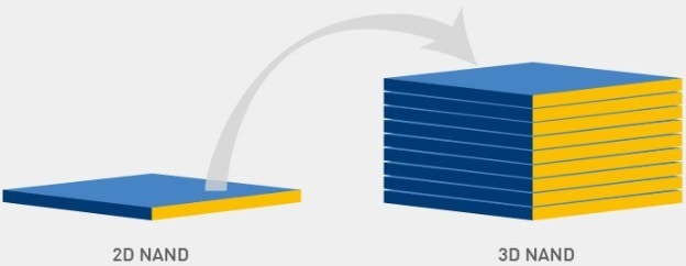
Firstly, 2D NAND: In mathematics and physics, 2D and 3D refer to dimensions or directions, specifically pertaining to coordinate axes. “2D” refers to the length and width on a flat plane, while “3D” adds the concept of “height” in a perpendicular direction to the 2D plane.
In the context of NAND technology, 2D NAND essentially represents the arrangement of chips within a single die, following the traditional two-dimensional flat-plane pattern for arranging flash chips.
On the other hand, 3D NAND innovates upon the 2D NAND by arranging chips not only in the two-dimensional plane but also in the vertical direction, effectively stacking chips in addition to the traditional flat-plane stacking.
The utilization of this new technology, 3D NAND technology, allows for chips to be stacked in a three-dimensional manner, overcoming the limitations posed by the physical limits of wafers. It significantly increases the capacity volume of flash chips per die within the same physical size, thereby pushing forward the overall capacity of storage chips.
In the industry, 3D NAND chips can be further categorized based on the number of layers stacked vertically and the type of chips used. This results in different products such as 32-layer, 48-layer, or even 64-layer 3D TLC/MLC chips. The choice depends on the technological capabilities and the specific chip types adopted by major original equipment manufacturers.
To better understand the difference and connection between 2D NAND and 3D NAND technologies, we can draw an analogy:
2D NAND is akin to building single-story houses on a limited flat surface. These houses are neatly arranged, but as demand grows, the number of houses multiplies. Eventually, this finite flat surface can only accommodate a certain number of houses and cannot be further expanded.
On the other hand, 3D NAND is like constructing multi-story buildings on the same flat surface. Within the same physical area, the volume efficiency of these buildings far surpasses that of single-story houses. Consequently, they provide more space, which translates to greater storage capacity. The designations of 32-layer, 48-layer, and 64-layer refer to the height of these buildings, indicating how many layers have been stacked vertically.
Bonus Reading: Performance Metrics for Solid-State Drives (SSDs) #
Sequential Read and Write (Seq) #
Sequential read and write operations are common tasks in daily computer usage, such as copying and transferring data. These processes involve reading and writing data in an organized sequence. Therefore, the sequential read speed of most SSDs is typically quite fast.
4K Random Read and Write (4K) #
4K random read and write typically refers to the read and write speeds at the system level, such as when booting up the system or launching software applications. These operations involve reading and writing small, non-sequential data because the data accessed during these operations is often unstructured and small in size, with 4KB being the minimum data block size in an uncompressed system. Therefore, 4K random read and write performance serves as a benchmark for assessing system responsiveness. Faster 4K read and write speeds indicate smoother system operation, which, in turn, reflects the SSD’s performance.
Access Latency (Access Time) #
Access latency typically refers to the time required for the system to access data from a storage device. In general, SSDs have access latencies that are below 1 millisecond, which is approximately a thousand times faster than traditional mechanical hard drives. This is one of the significant reasons why we experience substantial performance improvement when using SSDs as system drives. Higher-end SSDs tend to have even lower access latencies.
IOPS (Input/Output Operations Per Second) #
IOPS refers to the number of I/O (input/output) requests that a system can handle within a unit of time, typically measured in I/O requests per second (IOPS/s). A higher IOPS value indicates faster system processing speed and stronger SSD performance.
What Capacity is appropriate? #
In the case of YUNZE NVMe SSDs with the same materials used, the 128GB version has a write speed of only 600MB/s, while the 256GB version achieves nearly double that speed at 1100MB/s.
The controller allocates storage tasks reasonably among the flash memory chips to ensure that each unit’s workload is evenly distributed. This prevents overloading a specific unit, as more units lead to a reduced workload per unit. As a result, larger capacity drives have fewer tasks distributed evenly among them, naturally extending their lifespan.
128GB: It’s best to avoid this capacity as these drives typically have the lowest performance due to fewer memory modules. After installing the operating system, they can’t handle much, and upgrading to the next level doesn’t usually cost much more.
250GB: This capacity is often used in basic laptop configurations and is sufficient for everyday office tasks. If you’re on a tight budget, you can also combine it with an HDD, but a 500GB drive is recommended.
500GB: This offers the best value for money. Although 1TB might be more appealing, 500GB strikes a good balance between price and capacity. You can use an HDD for storing games and large files or delete them when you’re done.
1TB: If you’re an enthusiast needing to store a large amount of files or games, 1TB, 2TB, or 4TB drives are all suitable options. There’s no upper limit for those with high storage needs.

Recommended Reading:


