
Etching of Silicon Materials in Semiconductor Etching Processes: Gas Selection and Applications for Monocrystalline and Polycrystalline Silicon
Semiconductor manufacturing forms the foundation of the modern electronics industry, and etching processes are among the most critical steps in semiconductor fabrication. Among the many semiconductor materials, monocrystalline silicon and polycrystalline silicon are the most commonly used silicon-based materials, widely applied in integrated circuits, photovoltaic cells, sensors, and other fields. This article provides a detailed overview of the gas selection, reaction mechanisms, and optimization strategies for these two materials in etching processes, offering a comprehensive understanding of key aspects of semiconductor etching technology.
01
Overview of Monocrystalline and Polycrystalline Silicon Etching
Although monocrystalline and polycrystalline silicon are both silicon materials, their differing crystal structures result in distinct characteristics during etching processes. Monocrystalline silicon features a highly ordered atomic arrangement and a complete crystal structure, commonly used as the substrate for high-performance semiconductor devices. Polycrystalline silicon consists of many small crystal grains with numerous grain boundaries, often used in components such as gates and capacitor electrodes. These two materials require different gas choices, etching rates, and sidewall morphology control during the etching process.
Etching processes are mainly categorized into wet etching and dry etching. Wet etching uses chemical solutions (e.g., hydrofluoric acid, nitric acid) for isotropic material corrosion, suitable for processing flat surfaces. However, as device sizes continue to shrink, dry etching—especially reactive ion etching (RIE)—has become the mainstream technology due to its superior anisotropy (vertical etch rate much higher than lateral) and pattern fidelity.
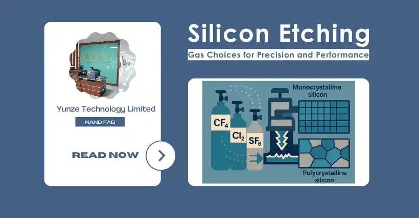
In dry etching, gas selection is a key factor in determining the etching outcome. Commonly used etching gases include fluorine-containing gases (e.g., SF₆, CF₄), chlorine-containing gases (e.g., Cl₂), and bromine-containing gases (e.g., HBr). These gases decompose in plasma environments to produce reactive radicals and ions, which react chemically or physically bombard silicon materials to precisely remove them. The following sections examine the gas selection and characteristics for monocrystalline and polycrystalline silicon etching.
02
Gas Selection for Monocrystalline Silicon Etching
Monocrystalline silicon etching is primarily used for wafer thinning, deep trench etching (such as DRAM capacitor structures), and MEMS device fabrication. Due to its uniform crystal structure, monocrystalline silicon etching typically requires high etching rates and good profile control.
Sulfur hexafluoride (SF₆) is one of the most commonly used gases for monocrystalline silicon etching. SF₆ decomposes in plasma to generate fluorine radicals (F), which react with silicon to form volatile SiF₄, enabling rapid material removal. SF₆ etching features fast rates and good anisotropy, suitable for high-efficiency applications. However, pure SF₆ etching can cause sidewall undercutting (i.e., excessive lateral etching), so it is often mixed with other gases in practical applications to enhance anisotropy.
Carbon tetrafluoride (CF₄) is another commonly used fluorine-containing etching gas, with a mechanism similar to SF₆ but a lower etch rate. CF₄ offers better process controllability and can be mixed with oxygen (O₂) to adjust the etch selectivity (the rate difference between materials). For example, in cases requiring silicon etching while preserving silicon dioxide (SiO₂), CF₄/O₂ mixtures provide better selectivity.
For applications requiring extremely high aspect ratios (e.g., over 10:1, such as through-silicon vias, TSV), the Bosch process is widely adopted. This process alternates between chemical etching with SF₆ and passivation with C₄F₈, forming high aspect ratio structures through cyclic steps. This approach combines high-speed etching with effective sidewall protection.
03
Gas Selection for Polycrystalline Silicon Etching
Polycrystalline silicon is mainly used as gate material, interconnect layers, and capacitor electrodes in semiconductor devices. Compared to monocrystalline silicon, polycrystalline silicon etching faces more challenges, particularly grain boundary effects that may cause etch non-uniformity and photoresist erosion. Therefore, polycrystalline silicon etching generally requires higher anisotropy and better sidewall protection mechanisms.
Chlorine gas (Cl₂) is a traditional mainstream gas for polycrystalline silicon etching. Chlorine radicals generated in Cl₂ plasma react with silicon to form volatile SiCl₄, achieving high etching rates. However, pure Cl₂ etching has poor anisotropy and tends to cause sloped sidewalls. To improve verticality, oxygen (O₂) or helium (He) is often added. O₂ forms SiOₓClᵧ protection layers on sidewalls during etching to suppress lateral etching, while He increases plasma density and enhances ion bombardment effects.
Hydrogen bromide (HBr) plays an increasingly important role in modern polycrystalline silicon etching. Compared to Cl₂, HBr’s biggest advantage lies in its sidewall protection ability. HBr reacts with silicon to form large amounts of SiBrₓ polymers that deposit on sidewalls as a protective layer, effectively preventing undercutting. A recent patent by Zhejiang Xinchip Semiconductor Technology uses a combination of HBr as the main etching gas and SF₆ as an auxiliary, achieving excellent anisotropy while significantly improving polycrystalline silicon trench morphology. However, HBr’s drawback is its slower etch rate, so a small amount of SF₆ or Cl₂ is often added to improve efficiency.
For applications requiring high selectivity (e.g., etching polycrystalline silicon while preserving the underlying silicon nitride), HBr/Cl₂/O₂ gas mixtures perform excellently. Experimental data shows that the appropriate ratio of HBr can result in a polycrystalline silicon to silicon nitride etch selectivity as high as 23:19. This high selectivity is particularly important for gate etching in advanced IC manufacturing, effectively preventing damage to underlying layers.
04
Etching Process Optimization and Challenges
In actual semiconductor production, relying solely on one gas is often insufficient to meet all requirements, making gas combinations and process parameter optimization essential. Etch rate, selectivity, anisotropy, and residue control are four key indicators for evaluating an etching process.
RF power is an important parameter influencing etch outcomes. Increasing RF power raises plasma density and accelerates etching, but excessive power can intensify ion bombardment, lowering etch selectivity (e.g., poly-Si to SiN) and increasing photoresist erosion. Experiments show that in Cl₂/He etching, raising RF power from 75W to 200W increases the polycrystalline silicon etch rate from ~100nm/min to 300nm/min, but reduces SiN selectivity from 15:1 to 5:19.
Adjusting gas ratios is another common optimization method. In the HBr/Cl₂/O₂ system, increasing O₂ flow enhances the etch rate and selectivity of polycrystalline silicon, as O₂ forms SiOxCly with SiClₓ and increases reactive Cl concentration. O₂ also reacts with silicon nitride to form a SiOxNy protective layer that suppresses its etching. While adding HBr reduces etch rate, it significantly improves sidewall morphology and selectivity.
Etching residue is another important challenge. After etching polycrystalline silicon with HBr/Cl₂/He-O₂ mixtures, silicon oxide residue layers often form on the surface. Studies show that these residues severely affect subsequent processing steps and device performance and must be removed by wet cleaning (e.g., O₃/H₂SO₄ solutions) or dry cleaning (e.g., O₂ plasma). XPS analysis confirms that wet cleaning is more effective in achieving clean surfaces than dry methods.
05
Application Examples and Future Trends
The choice of etching processes for different silicon materials ultimately depends on the specific application. In photovoltaic cell manufacturing, the textured surface of monocrystalline silicon (used to reduce light reflection) typically uses anisotropic wet etching with NaOH or KOH solutions, while localized rear contacts in high-efficiency PERC cells require precise patterning via dry etching.
In integrated circuits, polycrystalline silicon gate etching is a key technology. As transistor sizes shrink to the nanoscale, traditional Cl₂-based etching has gradually been replaced by HBr-based processes to achieve more vertical sidewalls and smaller linewidth deviations. A recent patent by NAURA showcases a “unique combination of etching and passivation gases” that achieves uniform etch rates across dense and sparse pattern regions, significantly improving FinFET performance.
3D NAND flash memory is another typical application, with stacked structures reaching 128 layers or more, requiring extremely high aspect ratios and uniformity. In such cases, the Bosch process—alternating SF₆ etching and C₄F₈ passivation—can achieve aspect ratios exceeding 40:1. Although aimed at metal etching, the latest aluminum mask technology from GTA Semiconductor—which uses polymer control to regulate plasma density—may also inspire improvements in silicon etching.
Looking ahead, semiconductor etching technology will evolve toward higher precision, higher selectivity, and lower damage. Atomic Layer Etching (ALE), which achieves atomic-level removal precision, may represent the next breakthrough in etching processes. Meanwhile, increasing environmental regulations make the development of green etching gases (with low Global Warming Potential, GWP) a pressing issue. Additionally, the application of artificial intelligence and machine learning in etching process optimization is expected to further boost productivity and yield.
06
Conclusion
As foundational materials in the semiconductor industry, monocrystalline and polycrystalline silicon require careful etching process selection and optimization to ensure device performance and control manufacturing costs. From traditional Cl₂ and SF₆ gases to modern HBr-based mixtures, etching technologies continue to evolve to meet increasingly demanding fabrication requirements. Understanding the properties and interactions of different gases, combined with application-specific parameter optimization, is key to achieving ideal etching results. As semiconductor technology progresses to ever-smaller nodes, etching processes will remain essential, and innovations in gas chemistry and equipment technology will open new possibilities.
Related:
- Etching Alumina: Key Gases Used in Semiconductor Industry
- Key Etching Gas Requirements in Semiconductor Process
- Key Differences in Three Silicon Wafer Orientations
- Understanding Chamfering in Semiconductor Processes

Disclaimer: This article is created by the original author. The content of the article represents their personal opinions. Our reposting is only for sharing and discussion purposes and does not imply our endorsement or agreement. If you have any objections, please get in touch with us through the provided channels.