
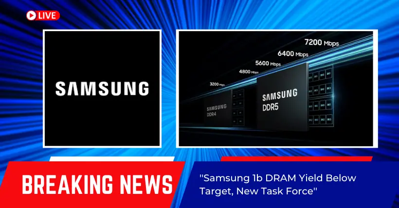
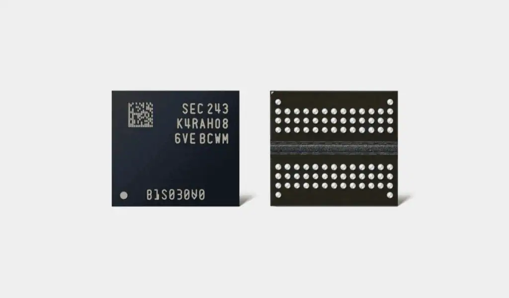
The yield rate of Samsung’s fifth-generation 10-nanometer-class (1b) process DRAM memory has not reached the industry’s general target of 80% to 90%. This has led Samsung to establish a dedicated task force last month to address the issue.
In May 2023, Samsung announced the mass production of fifth-generation 10-nanometer-class (1b) process 16Gb DDR5 memory, and in September 2023, it announced the successful development of fifth-generation 10-nanometer-class (1b) process 32Gb DDR5 memory. This indicates that Samsung can produce high-density 128GB DDR5 RDIMM memory modules without using TSV (Through-Silicon Via) technology.
Compared to 3DS DIMM memory using TSV technology, these memory modules without TSV technology reduce power consumption by 10% and significantly lower manufacturing costs. Therefore, Samsung Electronics regards the fifth-generation 10-nanometer-class (1b) process 32Gb DDR5 memory chips as a main product for the future. Now, Samsung has formed a dedicated task force to quickly improve yield rates to enhance market competitiveness.
Samsung Electronics has also decided to actively expand the production of the fifth-generation 10-nanometer-class (1b) process DRAM. The Hwaseong 15 and Pyeongtaek P2 fabs will become the main production bases for this product. Currently, the Pyeongtaek P2 fab primarily produces third-generation 10-nanometer-class (1z) process memory and will undergo a process technology upgrade in the future.
Related:
- Samsung DRAM Redesign Aims for Higher Yields by 2025 Q2
- IBM and Rapidus Partner to Develop 2nm Chip Technology

Disclaimer: This article is created by the original author. The content of the article represents their personal opinions. Our reposting is for sharing and discussion purposes only and does not imply our endorsement or agreement. If you have any objections, please get in touch with us through the provided channels.