
Before the PCB design is completed and moves on to the PCB production stage, there is one crucial step left unfinished, which is PCB panelization. Panelization is sometimes provided by the customers themselves, and at times, it is completed by the engineers at the PCB manufacturing facility and then given to the customer for confirmation. Once confirmed without errors, it can then be put into production.
PCB panelization not only involves the quality of the PCB circuit board but also has a significant impact on the cost of PCB production. How to effectively panelize while ensuring the quality of the PCB circuit board, thereby saving raw materials, is a matter that PCB design companies and manufacturers need to pay special attention to.
01
What is PCB Panelization?
Today’s electronic products are increasingly moving towards being compact and lightweight. When you design PCB circuit boards that are extremely small, some electronic product modules are as small as a few square centimeters, and PCB fabrication is not a major concern. However, when it comes to the PCB assembly process, the challenge arises when placing such small PCBs onto assembly machines, making it impossible to use the assembly production line.
This is where PCB panelization comes into play. It involves joining small PCBs to create an appropriate area that meets the requirements for machine assembly or creating panels with both positive and negative sides, making it easier for surface mount assembly. In most cases, PCB manufacturers offer panelization services.
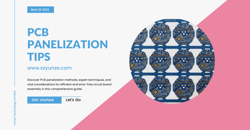
PCB panelization is the process of combining multiple individual PCBs (boards with no electrical connections between them) into a single board for production. This allows for the simultaneous production of multiple board types, which is faster and often more cost-effective than producing individual PCBs.
However, it’s important to note that PCB panelization requires that the layers and manufacturing processes of the boards being panelized are consistent; otherwise, panelization is not possible.
02
PCB Panelization Terminology Explanation
① Mark Points
Mark points are used to assist in the optical positioning of SMT (Surface Mount Technology) pick-and-place machines for PCBs with SMT components. In a PCB board, there should be at least two asymmetric reference points at the diagonally opposite corners to facilitate optical alignment. For whole PCBs, reference points are generally placed at corresponding positions on the diagonal corners of the entire PCB. For divided PCBs, reference points are typically located at corresponding positions on the diagonal corners of the divided PCB. In the case of devices with a lead pitch of ≤0.5mm for QFP (Quad Flat Package) square and flat packages and a ball pitch of ≤0.8mm for BGA (Ball Grid Array) ball grid array packages, it is required to set reference points at the two diagonally opposite corners of the IC (integrated circuit) to enhance pick-and-place accuracy.
② Process Edge
Process edges refer to the additional sections added to the sides or corners of a PCB board to assist in the production of through-hole components, wave soldering, or other manufacturing processes. These sections are primarily intended to aid in the manufacturing process and are not considered part of the PCB. Once production is complete, these sections are typically removed.
03
Why is Panelization Necessary Before PCB Production?
There are two primary reasons for PCB panelization:
① Cost Savings and Convenience for PCB Manufacturers
PCB production typically starts with Copper-Clad Laminate (CCL), which serves as the foundational material for the PCB manufacturing process. CCL sheets are typically produced in standardized sizes. However, the specifications of PCBs can vary significantly from one customer to another. PCBs come in various sizes, shapes, and dimensions. Panelization of PCBs becomes essential to maximize the efficient utilization of CCL sheets and reduce the cost of raw materials. This process allows multiple PCBs to be fabricated from a single CCL sheet of the same size, which is cost-effective.
② Facilitating Subsequent SMT (Surface Mount Technology) assembly
After PCB fabrication, electronic components need to be placed on the PCB through SMT assembly. Each SMT assembly facility may have specific requirements for the size and dimensions of the PCBs to be used on their assembly lines. If the PCB size is either too small or too large, it can cause issues with the fixtures that hold the PCBs in place during assembly. In cases where the PCB size is smaller than the factory’s specified requirements, panelization is necessary. By combining multiple smaller PCBs into a single larger panel, the efficiency of high-speed pick-and-place machines and wave soldering processes can be significantly improved.
04
Methods for PCB Panelization
There are primarily three methods for PCB panelization: V-CUT, scoring, and perforated holes (mouse bites). The choice of panelization method depends on the size of the PCB. Panelization is typically used when the PCBs are neither too large nor too small. Very small boards can be panelized for ease of processing or soldering.
1. V-Cut
The V-Cut method involves cutting a V-shaped groove at the edge of the board and then bending the board to separate it. This approach allows for a clean and precise separation of individual boards. V-Cut is widely used for creating individual PCBs or separating PCBs with a standardized design.
2. Copper Foil Bridge
The Copper Foil Bridge method reserves some protruding parts on the board, which can be used to connect multiple boards together for interconnection. This method offers flexibility in creating complex PCB layouts with interconnected sections, ideal for custom applications.
3. Separable Interconnection
Separable Interconnection involves leaving small connecting points between the boards and then separating the boards by breaking these connecting points. This method is suitable for designs that require easy separation and reconnection, such as modular electronics.
4. Panelization
Panelization is a method that involves placing multiple PCB designs on a large substrate and then using mechanical or V-Scoring methods to separate them. It is often used for mass production of small PCBs on a larger panel, allowing for efficient manufacturing.
Knowing these four PCB interconnection methods, I believe you will be able to use them flexibly. If you are still unclear, we will provide you with information on the uses and advantages of PCB interconnection methods.
05
Requirements for PCB Panelization Process
- In the case of irregular PCB panelization, there should be no gaps on either side of the panel, and corners must not have cutouts (at least one side should be uncut). Otherwise, the positioning pins of SMT machines cannot locate the panel, leading to difficulties in component placement.
- For double-sided PCBs, it’s essential to pay attention to the differentiation between Plated Through Holes (PTH) and Non-Plated Through Holes (NPTH).
06
Advantages of PCB Interconnection
PCB interconnection offers several advantages that significantly impact the manufacturing process and the quality of electronic products:
1. Improve Production Efficiency
Interconnection can combine multiple PCB designs, reducing manufacturing time and labor costs through batch processing, especially in large-scale production. This results in quicker turnaround times and cost savings for manufacturers.
2. Reduce Manufacturing Costs
Interconnection maximizes the use of raw materials and minimizes waste production. Additionally, it reduces processing steps and equipment usage, helping to lower manufacturing costs. This makes it a cost-effective solution for electronics production.
3. Facilitate Assembly and Testing
Interconnection technology simplifies and streamlines the assembly process. Multiple PCBs can undergo component installation and wiring simultaneously, reducing assembly time. Moreover, interconnection aids in rapid batch testing and debugging, speeding up the entire production process.
4. Enhance Product Quality and Reliability
Using interconnection, you can ensure precise and error-free connections and alignment between multiple PCBs, reducing the risk of faults caused by poor connections or misalignment of circuits. Furthermore, interconnection provides better electrical and mechanical stability, which is essential for the reliability of electronic devices.
5. Ease of Maintenance and Repair
If multiple PCBs are integrated on a single interconnect board, maintenance and repair only require handling the entire unit, saving time and effort. This simplifies the servicing of electronic devices, which is essential for product longevity.
07
Ten PCB Panelization Techniques
- The outer frame (clamping edge) of PCB panelization should feature a closed-loop design to ensure that the PCB remains fixed in the fixture without deformation. Typically, V-grooves are not allowed on this edge.
- The width of the PCB panel should be ≤260mm (for SIEMENS lines) or ≤300mm (for FUJI lines), depending on the production line. Exceeding the module’s range may significantly slow down the processing speed. If automatic soldering is required, the PCB panel’s width × length should be ≤125mm × 180mm.
- The shape of the PCB panel should closely resemble a square, and it is recommended to use panelization patterns like 2×2, 3×3, etc., but avoid creating positive and negative panels.
- The center-to-center spacing between smaller PCBs should be controlled within the range of 75mm to 145mm.
- When setting reference positioning points, at least three or more positioning points should be placed along the edge of the PCB. These points are essential for ensuring the board’s position and level. Leave an unmasked area around the positioning points, typically 1.5mm larger than the point’s size. It’s best to place these points 5mm from the edge, and the spacing between them should be different when the travel direction is not consistent (for ease of direction differentiation).
- For component placement, ensure that all orientations are consistent to avoid mirror-image issues, which can cause problems with coordinate positioning. Additionally, there should be no connectors extending from the edges (between the panel’s outer frame and internal smaller boards or between smaller boards). Such connectors can hinder tool separation after soldering.
- Four positioning holes with a diameter of 4mm ± 0.01mm should be placed in the four corners of the PCB panel’s outer frame. These holes should have moderate strength to prevent breakage during upper and lower board processes. The accuracy of hole size and positioning should be high, and the hole walls should be smooth without burrs.
- Each small board within the PCB panel should have at least three positioning holes with a diameter ranging from 3mm to 6mm. No wiring or components are allowed within 1mm of the edge positioning holes to prevent misjudgment.
- For whole board positioning on PCBs and for precise spacing components, positioning symbols should be placed at diagonally opposite positions for QFPs with a pitch of less than 0.65mm. For PCB sub-panels used in panelization, positioning symbols should be used in pairs, positioned at the diagonal corners of the positioning elements.
- Large components should have positioning pins or holes, particularly for I/O interfaces, microphones, battery connectors, tactile switches, headphone jacks, motors, and other significant components.
08
Additional Considerations for PCB Panelization
① Leave Space and Create Slots in PCB Panelization
Leaving space and creating slots during PCB panelization serve specific purposes. Leaving space provides a designated area for future component soldering or surface mounting, ensuring a secure location for these processes. Slots, on the other hand, are designed to separate individual PCBs from the panel. The recommended space or border width is typically within the range of 2-4mm. When placing components on the PCB, this border should be based on the maximum component width. Slot creation involves specifying areas where no wiring or material layers are allowed to pass through. The specific details of slot placement and processing should be discussed and agreed upon with the PCB manufacturer, with clear instructions provided by the design team. PCB panelization aims to streamline production and improve efficiency, and the method of space and slot creation can be chosen based on individual preferences.
② V-Cuts and Slots as Methods for Milling PCB Profiles
Both V-cuts and slots are ways to mill the profiles of PCBs during panelization. These methods make it easy to separate multiple boards, reducing the risk of damaging the circuit boards during separation. The choice between V-cuts and slots should be based on the shape and requirements of the specific product being panelized. V-cuts are suitable for straight-line separation and may not be ideal for panelizing boards with varying dimensions.
③ Panelization Requirements
Typically, the number of different PCB types to be panelized should not exceed four. Each type of board should have the same number of layers, copper thickness, and surface finish requirements. Additionally, it is advisable to consult with the PCB manufacturer’s engineers to determine the most rational panelization strategy.
Panelization is done to save costs, but if the production process is complex or the batch size is large, it may be more practical to produce the boards separately. It’s important to note that panelization may also involve a waste rate ranging from 10% to 20%, depending on the specifics of the production.
09
Frequently Asked Questions (FAQs)
Q1. What is the purpose of PCB interconnection?
PCB interconnection is essential to connect multiple circuit boards effectively, enabling seamless communication between different components in electronic devices.
Q2. Which PCB interconnection method is best for small-scale production?
For small-scale production, V-Cut and Copper Foil Bridge methods are often the preferred choices, as they offer precise separation and flexibility in design.
Q3. How does PCB interconnection reduce manufacturing costs?
Interconnection maximizes material usage, minimizes waste, and streamlines the manufacturing process, leading to cost savings.
Q4. Can PCB interconnection be used for repairing electronic devices?
Yes, PCB interconnection simplifies maintenance and repair by allowing for the handling of multiple PCBs as a single unit.
Q5. What are the key considerations when choosing a PCB interconnection method?
Consider the production scale, design complexity, and ease of maintenance when selecting the most suitable PCB interconnection method for your project.
Related:
- Improve PCB Cooling Easily with Smart Design Ideas
- How to do PCBA Testings and what essential equipment
- PCB Lamination Process: Key Steps and Techniques

Disclaimer: This article is created by the original author. The content of the article represents their personal opinions. Our reposting is for sharing and discussion purposes only and does not imply our endorsement or agreement. If you have any objections, please contact us through the provided channels.