
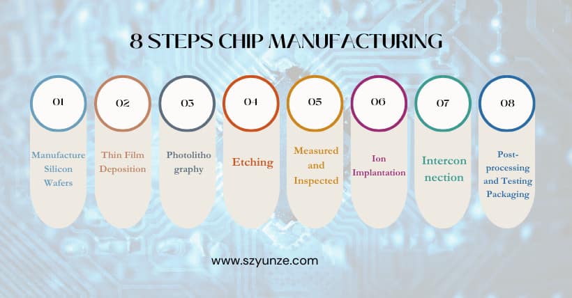
Throughout the entire manufacturing industry, the manufacturing process of chips can be said to be one of the most complex. This alchemical art can be divided into eight major steps, as shown in the diagram Above, and these steps can be further subdivided into hundreds of processes.
01
Manufacturing Silicon Wafers
The raw material for manufacturing silicon wafers is the common sand, primarily composed of silicon dioxide. By purifying sand, we obtain elemental silicon. This elemental silicon is then used to produce single-crystal silicon ingots through the Czochralski method. The silicon ingot is initially cut at both ends and then into several segments, followed by grinding to achieve the standard diameter for the single-crystal silicon rod.
Subsequently, X-ray diffraction is employed to determine the crystal orientation of the single-crystal silicon. A reference plane is removed, and cutting is carried out based on this reference plane to produce silicon wafers, as illustrated in the diagram below.
After obtaining the preliminary wafer, the cut silicon wafer needs to undergo chamfering and grinding processes to make its surface smooth and even. Otherwise, it would be challenging to accurately etch circuits on it. After grinding, the chemical etching solution is used to remove any damage incurred during the grinding process. Finally, a polishing solution is applied. Once it passes inspection, it can be handed over to the production line for further manufacturing.
02
Film Deposition
Steps two through six involve processes that need to be repeated multiple times. Film deposition is the process of depositing thin film materials onto the surface of the wafer. The materials for deposition can be conductors, semiconductors, or insulators. Common types of thin films include silicon dioxide, polycrystalline silicon, silicon nitride, and various metal and compound films. Common deposition methods include Chemical Vapor Deposition (CVD) and Physical Vapor Deposition (PVD).
CVD involves introducing vaporized reactants, either gaseous or liquid, that make up the thin film material into a reaction chamber at a controlled flow rate. Chemical reactions occur on the substrate surface, leading to film deposition, as shown in the diagram below.
Physical Vapor Deposition (PVD) is a process conducted under vacuum conditions. It involves using physical methods to vaporize the material source (solid or liquid) into gaseous atoms or molecules or partially ionize them into ions. These species are then transferred to the silicon substrate surface, forming the thin film, as depicted in Figures 3-5. Compared to CVD, PVD has the advantage of a simpler process principle and lower required process temperatures, making it suitable for various film preparations. However, PVD films may exhibit poorer step coverage, adhesion, and density compared to CVD films.
Common types of PVD include sputter deposition, vacuum evaporation, and plasma deposition. Take sputter deposition as an example; it involves creating a certain level of vacuum, ionizing the gas, and bombarding the target material surface with ions. The particles from the target material surface are transferred to the substrate, resulting in film deposition, as shown in the diagram below.
03
Photolithography
Photolithography is the most crucial step in the entire manufacturing process. Before photolithography, a uniform layer of photoresist is applied to the wafer’s surface. Typically, photoresist is applied using a spinning method, where it is spread while spinning to ensure even coverage, as shown in the diagram below.
After applying the photoresist, the wafer is placed into a photolithography machine. The machine’s light source emits deep ultraviolet (DUV) or extreme ultraviolet (EUV) light, which passes through a mask, also known as a photomask. This light reduces and focuses the circuit pattern from the photomask onto the photoresist layer. When the photoresist is exposed to light, a chemical change occurs in the exposed areas. The circuit pattern from the photomask is transferred onto the photoresist layer in this step, known as exposure, as shown in the diagram below.
Following exposure, the next steps involve baking and developing. These steps aim to remove the photoresist in the areas not exposed to light, revealing the printed circuit pattern and permanently fixing it in place.
04
Etching
Etching is the process that occurs after the photolithography step, where unwanted materials are selectively removed from the silicon wafer’s surface using chemical or physical methods, leaving behind the 3D circuit pattern. Etching methods primarily include wet etching and dry etching.
Wet etching involves the use of a chemical solution to remove the material not protected by the masking material through a chemical reaction, achieving the etching goal.
Dry etching, on the other hand, is a technique that utilizes highly chemically reactive properties of plasma to etch thin films. Dry etching methods include sputter etching, plasma etching, and reactive ion etching (RIE). As an example, in the case of plasma etching, particles in the plasma collide with the silicon dioxide thin film layer, effectively removing excess oxide layers, as shown in the diagram below.
05
Metrology and Inspection
After the etching process, the wafer undergoes metrology and inspection to ensure there are no errors. If the inspection results do not meet expectations, feedback is provided to the photolithography or etching steps for further optimization and adjustments. In fact, metrology and inspection are integral throughout the entire manufacturing process.
06
Ion Implantation
Ion implantation involves accelerating atoms (such as elements from groups III and V) to specific regions of the wafer under the influence of a strong electric field. This is followed by steps like annealing, impurity activation, and lattice damage repair to achieve the desired impurity concentration. Ultimately, this process forms either an N-region or a P-region.
07
Interconnection
Interconnection refers to the technique of connecting various independent components within the same chip to form a circuit module with specific functionality. The metal materials used for interconnection processes need to have characteristics such as low resistivity, good thermal and chemical stability, excellent resistance to electromigration, ease of deposition and etching, and cost-effectiveness. In the early stages of integrated circuit development, aluminum interconnection technology was primarily used. However, copper, due to its lower resistivity and better resistance to electromigration, has been widely adopted.
From film deposition to interconnection, these six steps are repeated dozens or even hundreds of times throughout the entire manufacturing process. Each repetition involves the fabrication of a layer of circuits on the wafer, ultimately resulting in a complete chip. After completing all of the aforementioned steps, the wafer undergoes processes like grinding, polishing, testing, and packaging. The qualified chips are then ready for delivery from the factory!
Related:

Disclaimer: This article is created by the original author. The content of the article represents their personal opinions. Our reposting is for sharing and discussion purposes only and does not imply our endorsement or agreement. If you have any objections, please contact us through the provided channels.