
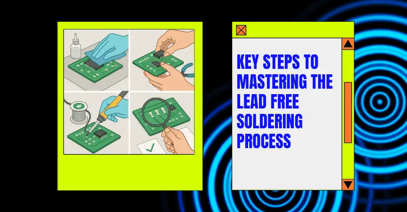
The core steps of the lead-free soldering process are as follows, with each step including key control points to ensure soldering quality:
01
Pre-soldering Preparation Optimization
Automatic Optical Inspection (AOI) equipment is introduced to perform preliminary checks on component leads and PCB pads, reducing the time required for manual inspection.
Ion contamination testers are used to check PCB cleanliness, ensuring compliance with the low contamination requirements of the lead-free process.
A solder paste inventory management system is established, following the First-In-First-Out (FIFO) principle to prevent waste from expired solder paste.
02
Solder Paste Printing Optimization
Laser nano-coated or electroformed stencils are used, with nano-level polishing of aperture edges to reduce solder paste residue.
An online stencil thickness inspection system is introduced to ensure thickness deviation is controlled within ±2μm.
A closed-loop control system is used to monitor and adjust key parameters such as printing pressure, speed, separation distance, and separation speed in real time.
An SPI machine vision system is deployed to detect solder paste deposition in real time, with automatic alarm triggered when deviation exceeds 5%.
03
Component Placement Optimization
Multi-axis placement machines are upgraded to achieve placement speeds of 80,000 CPH (components/hour) while maintaining high accuracy of ±30μm.
Vacuum nozzle pressure online monitoring technology is used to ensure stable component placement pressure, preventing solder paste extrusion.
Intelligent feeders are introduced to automatically switch component reels based on the BOM, significantly reducing line change time.
04
Reflow Soldering Optimization
Reflow ovens with adaptive learning functions are used to automatically adjust temperature settings in each zone based on PCB thermal capacity differences.
Infrared and thermocouple combined temperature measurement systems are deployed for 3D visual monitoring of the oven’s internal temperature field.
Localized nitrogen protection technology is used to inject nitrogen only in the reflow zone, controlling oxygen content below 50ppm to enhance soldering quality.
05
Wave Soldering Optimization (if applicable)
Traditional wave soldering is replaced with selective wave soldering to reduce thermal shock to components and PCBs.
A dual-wave design (turbulent wave and smooth wave combined) is used to improve through-hole fill rate to over 95%.
A flux spray closed-loop control system is introduced to automatically adjust spray volume based on PCB size and aperture, ensuring even flux coverage.
06
Manual Soldering and Rework Optimization
Rework stations with temperature profile presets are equipped to automatically record and reproduce successful rework parameters.
Infrared thermal imaging is used to monitor the rework area in real time, preventing component or PCB damage from overheating.
07
Post-solder Cleaning Optimization
Cleaning machines with online pH monitoring are introduced to automatically add cleaning agents, ensuring ionic contamination levels remain below 1.5μg/cm².
Vacuum steam degreasing technology is used to reduce cleaning agent consumption by over 50% while improving cleaning efficiency.
08
Inspection and Testing Optimization
AOI equipment based on deep learning algorithms is deployed to improve defect recognition rate to 99.9% while reducing false alarm rate to below 0.1%.
3D X-ray inspection systems are introduced for quantitative analysis of BGA solder voids, with an accuracy of ±1%.
Flying probe testers are used for online electrical testing, increasing test points to 10,000 and reducing test cycle to 30 seconds per board.
09
Rework and Repair Optimization
Laser rework stations are introduced for non-destructive removal and replanting of micro components such as BGAs, improving rework efficiency and quality.
A rework process database is established to automatically match optimal rework parameters, increasing one-time repair success rate to over 95%.
By implementing the above optimization measures, the efficiency and quality of lead-free soldering processes can be significantly improved, while effectively reducing costs and environmental pollution. Enterprises can phase in these optimization solutions based on their actual production scale, product complexity, and investment budget. It is recommended to prioritize upgrading inspection equipment and process control systems for rapid improvement.

Disclaimer: This article is created by the original author. The content of the article represents their personal opinions. Our reposting is only for sharing and discussion purposes and does not imply our endorsement or agreement. If you have any objections, please get in touch with us through the provided channels.