
01
Overview of the Three Core Testing Stages (CP (Chip Probing), FT (Final Test), and WAT (Wafer Acceptance Test))
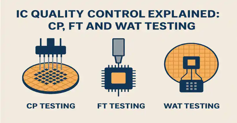
In the complex process of integrated circuit manufacturing, CP (Chip Probing), FT (Final Test), and WAT (Wafer Acceptance Test) constitute the key system for quality control. These three testing stages correspond to different phases of chip production, each with distinct objectives and targets. Like different components of a precision instrument, they work together to ensure the reliability and stability of chip products.
02
CP Test: Precision Filter at the Wafer Level
✅ Testing Role and Core Value
CP testing occurs at the initial stage of chip production, directly probing each individual die on the wafer surface. Through electrical performance tests, it accurately filters out chips that do not meet specifications and assesses the overall wafer yield. As a pre-packaging functional and electrical test, CP testing effectively prevents defective chips from entering subsequent packaging processes, significantly reducing production costs.
✅ Core Functions and Technical Challenges
Key functions of CP testing include:
- Precise Defective Chip Elimination
By measuring key electrical parameters such as threshold voltage (Vt), on-resistance (Rdson), and leakage current (Igss), unqualified chips are quickly identified and eliminated. - Process Monitoring and Optimization
It provides real-time feedback on the stability of wafer manufacturing processes, especially early-stage steps like lithography and deposition, offering data support for process adjustments.
In terms of technical challenges, the development of high-precision probe cards and test equipment is crucial—especially in high-current testing scenarios, which require exceptional equipment durability. At the same time, parallel testing of multiple dies on a wafer introduces signal interference issues, posing strict requirements on test accuracy control.
✅ Main Testing Items
CP testing focuses on basic electrical performance of chips, mainly covering:
- Threshold voltage (Vt)
- On-resistance (Rdson)
- Leakage current (Igss)
- Source-drain breakdown voltage (BVdss)
03
FT Test: The Final Quality Gate Post-Packaging
✅ Testing Stage and Core Objective
FT testing is the final inspection step in chip manufacturing, conducting comprehensive functional verification on finished, packaged chips. Its main objective is to ensure that chips perform reliably under real-world conditions and meet stringent design and application requirements.
✅ Core Functions and Implementation Challenges
Key tasks of FT testing include:
- Full-Scenario Functional Verification
Simulates chip operation under various working temperatures and voltage conditions to verify functional stability. - Packaging Impact Evaluation
Detects the potential impact of the packaging process on chip performance, especially in high-frequency and high-power applications.
During implementation, multiple challenges must be overcome: mechanical stress, thermodynamic changes, and electrical interference introduced during packaging require comprehensive environmental considerations during testing. Rigorous temperature testing standards such as “three-temperature testing” (room temperature, low temperature, high temperature) not only increase equipment costs but also lengthen testing cycles.
✅ Main Testing Items
FT testing covers multi-dimensional checks:
- Functional Testing
Verifies the accuracy of chip logic operations and functional implementation. - Environmental Adaptability Testing
Includes extreme condition testing such as thermal cycling and high humidity. - Electrical Performance Testing
Measures key indicators like current, voltage, and power consumption.
04
WAT Test: Guardian of Process Quality
✅ Testing Role and Core Function
WAT testing is conducted after front-end wafer processes and before wafer dicing and packaging. It tests specific structures on the wafer for electrical parameters to monitor process quality in real-time. This testing determines whether a wafer qualifies for the packaging phase and helps engineers foresee potential production line issues.
✅ Core Functions and Technical Challenges
WAT testing mainly serves two purposes:
- Process Stability Monitoring
Evaluates whether the wafer fabrication process meets standards by analyzing the electrical performance of test structures (e.g., Testkey). - Production Line Health Diagnosis
Uses feedback from test data to identify process variations and take corrective actions in advance.
Technically, it’s important to balance the design precision of test structures with wafer area usage to avoid reducing production efficiency. Also, the complex impact of different process steps on electrical parameters requires a refined quality control system.
✅ Main Testing Items
WAT testing mainly includes:
- Electrical Performance Measurement
Accurate measurement of voltage, current, and other parameters of wafer test structures. - Process Uniformity Evaluation
Analyzes samples from multiple regions to assess the stability and consistency of the fabrication process.
05
Comparison and Coordination Among the Three Major Tests
| Test Type | Core Objective | Test Target | Key Test Content | Core Technical Challenge |
|---|---|---|---|---|
| CP Test | Remove defective chips, monitor process | Individual dies on wafer | Basic electrical performance parameters | Probe card design, interference in parallel testing |
| FT Test | Verify functional reliability | Finished packaged chips | Full-function, environmental adaptability test | Packaging effect evaluation, temperature testing |
| WAT Test | Monitor process quality | Wafer test structures | Electrical performance, process uniformity | Test structure design, process effect control |
06
Conclusion: A Complete Quality Control Loop
CP testing reduces cost through early-stage filtering, FT testing ensures final product performance compliance, and WAT testing guarantees process stability from the source. Together, they form a complete quality control loop in integrated circuit manufacturing. Although some companies attempt to skip CP testing to simplify processes, its role in yield control remains irreplaceable, especially in high-precision and high-reliability fields. As a “barometer” of production line quality, WAT testing is a critical monitoring step throughout chip manufacturing. These three testing stages complement and reinforce each other, providing solid support for the high-quality development of the integrated circuit industry.
Related:

Disclaimer:
- This channel does not make any representations or warranties regarding the availability, accuracy, timeliness, effectiveness, or completeness of any information posted. It hereby disclaims any liability or consequences arising from the use of the information.
- This channel is non-commercial and non-profit. The re-posted content does not signify endorsement of its views or responsibility for its authenticity. It does not intend to constitute any other guidance. This channel is not liable for any inaccuracies or errors in the re-posted or published information, directly or indirectly.
- Some data, materials, text, images, etc., used in this channel are sourced from the internet, and all reposts are duly credited to their sources. If you discover any work that infringes on your intellectual property rights or personal legal interests, please contact us, and we will promptly modify or remove it.