
PCB and PCBA are the cornerstones of electronic products. In order to improve the yield rate, PCB manufacturers spare no effort to improve the manufacturing process and utilize various professional testing instruments to discover product defects. Today, SPEA wants to share the topic of how to test PCBA.
Many people may not fully understand the differences between PCB and PCBA. Before discussing how to test PCBA, let’s clarify the differences between the two.
1. What is PCB?
PCB, short for Printed Circuit Board, is often referred to as a bare board in the industry. It is an important component, serving as the support structure for electronic components and the carrier for electrical connections of electronic components.
2. What is PCBA?
PCBA stands for PCB Assembly, which refers to the circuit board obtained by mounting components on the PCB, including surface-mount technology (SMT) and through-hole technology (DIP). Simply put, it is a circuit board with resistors, integrated circuits, capacitors, and other components installed on it.
SMT (Surface Mounted Technology) is mainly used to mount small components onto PCBs without drilling holes, while DIP (Dual In-line Package) involves inserting components into pre-drilled holes on the PCB.
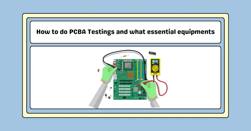
Now that we have a clearer understanding of PCB and PCBA, let’s move on to the main topic: what tests are conducted on PCBA circuit boards?
PCBA testing is the most critical quality control step in the entire PCBA manufacturing process, determining the final performance of the product. The main tests for PCBA include ICT (In-Circuit Test), FCT (Functional Circuit Test), aging test, and fatigue test.
- ICT testing mainly involves circuit continuity, voltage and current values, waveform characteristics, amplitude, noise, etc.
- FCT testing requires IC program burning to simulate the functionality of the entire PCBA board, identify hardware and software issues, and equip necessary fixtures and test benches.
- Aging test involves applying continuous power to PCBA boards and electronic products for a long time to observe any failures. Only after passing the aging test can electronic products be sold in bulk.
- Fatigue test samples PCBA boards and subjects them to high-frequency, long-term operations to observe failures and determine the probability of faults occurring during testing, providing feedback on the working performance of PCBA boards in electronic products.
3. What are common testing methods for PCBA?
① Manual Visual Inspection
This method involves visually inspecting the circuit and electronic components of the PCBA board using a magnifying glass. It checks for defects such as soldering bridges, excess solder, insufficient solder, and incomplete soldering. However, manual inspection is primitive and inefficient for mass production due to the increasing number and miniaturization of components on PCBs.
② AOI (Automated Optical Inspection)
AOI, also known as automated visual testing, utilizes specialized inspection equipment to check component polarity before and after reflow. However, optical inspection cannot test the physical performance of circuits, such as continuity.
③ ICT (In-Circuit Test)
In mass production factories, it’s impractical to manually measure every resistor, capacitor, inductor, or even IC circuit on each PCB board. Hence, the emergence of ICT (In-Circuit Test) automated testing machines. These machines use multiple probes, often referred to as “bed-of-nails” fixtures, to simultaneously contact all the component lines on the board. Then, through programmable sequences primarily based on a sequence, and parallel as secondary, it sequentially measures the characteristics of these electronic components.
However, there are limitations to using bed-of-nails fixtures for circuit testing. For instance, there is a minimum diameter limit for probes, as too small diameters can lead to bending or damage. There are also restrictions on the spacing between probes because each probe needs to come out of a hole, and the back end of each probe needs to be soldered to a flat cable. If adjacent holes are too small, besides the risk of short circuits between probes, interference from the flat cable can also be a significant issue.
Additionally, some high components may not be accessible for probing. If probes are too close to high components, there’s a risk of damaging them through collisions. Moreover, due to the height of the components, it’s usually necessary to create holes on the bed-of-nails fixture base to avoid direct contact, indirectly causing difficulty in probing all component test points on the circuit board.
④ Flying Probe Testing
Flying probe testing is widely regarded as a promising new testing technology that has the potential to replace bed-of-nails testing. Flying probe testers have rapidly advanced in terms of testing accuracy, speed, reliability, and coverage in recent years, and have become widely popular. Moreover, the increasing demand for rapid prototyping, small to medium production volumes of PCBs and PCBA, and the need for testing systems with quick setup and fixtureless capabilities highlight the flexibility and cost-effectiveness of flying probe testing.
The main advantages of flying probe testers include their ability to accelerate time-to-market for products, automatic test generation, absence of fixture costs, good diagnostic capabilities, and ease of programming. Advanced flying probe testers also integrate multiple practical functionalities such as 3D laser testing, programming, and boundary scanning.
⑤ MDA (Manufacturing Defect Analyzer)
MDA is a tool used for high-volume/low-mix environments, primarily for diagnosing manufacturing defects. It lacks digital drivers, so it cannot functionally test components or firmware on the board. MDA testing is faster than visual inspection but may struggle to keep up with production line speeds.
The PCBA manufacturing process is complex, and various product defect issues may arise during production. The selection of PCBA testing methods and equipment should be based on the specific characteristics of the PCBA.
Related:

Disclaimer: This article is created by the original author. The content of the article represents their personal opinions. Our reposting is for sharing and discussion purposes only and does not imply our endorsement or agreement. If you have any objections, please contact us through the provided channels.