
Common Structures in Advanced Packaging
| Structure Name | English Abbreviation | Description | Application Scenarios |
|---|---|---|---|
| Through-Silicon Via | TSV | Holes are made in silicon and filled with copper to vertically connect chips | 3D stacking, HBM, high-performance computing |
| Through-Glass Via | TGV | Similar to TSV but with glass as the substrate | High-frequency RF, SiP, substrate replacement |
| Cu Pillar | Cu Pillar | Fine-pitch interconnect between chip and substrate; electroplated copper with Sn cap | Flip Chip, FCBGA |
| Redistribution Layer | RDL | Redistributes chip I/O; usually multiple metal layers | Fan-Out, InFO, 2.5D packaging |
| Gold Bump | Au Bump | For gold wire bonding or TCB bonding | High-reliability packaging, optoelectronic chips |
| Micro Bump | µBump | Fine-pitch bumps (<30μm) for die-to-die interconnection | 2.5D, 3D-IC, HBM, Chiplet |
| Solder Ball | Solder Ball | For soldering to substrates | Used in almost all chip packaging |
The structures listed above are essentially the “core” of advanced packaging processes. Why electroplating is used instead of other metallization methods:
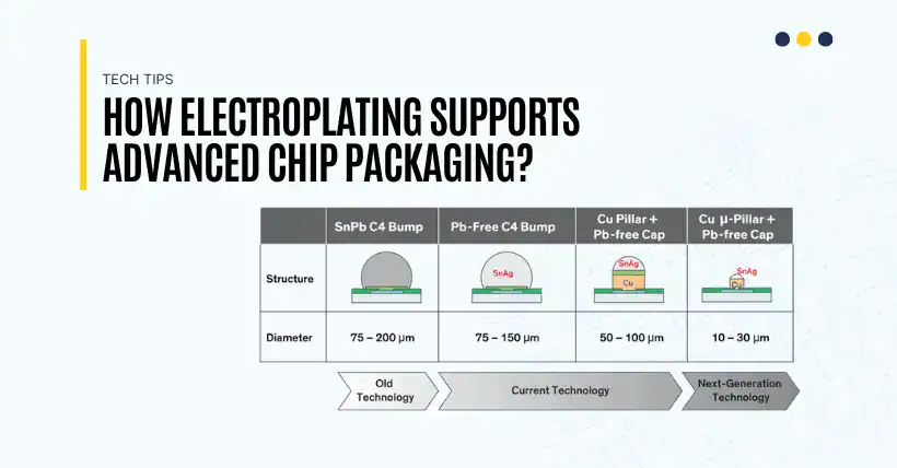
Take the cover image as an example: in advanced packaging, the structure height needs to reach at least several microns to several hundred microns. Only electroplating has a plating speed that can meet this requirement. At a current density of 1 ASD, the copper plating rate is 0.2 µm/min. Generally, the current density can be adjusted within a range of 1–15 ASD, so the plating rate can reach an impressive 3 µm/min. This is unattainable by typical PVD or CVD methods.

Disclaimer:
- This channel does not make any representations or warranties regarding the availability, accuracy, timeliness, effectiveness, or completeness of any information posted. It hereby disclaims any liability or consequences arising from the use of the information.
- This channel is non-commercial and non-profit. The re-posted content does not signify endorsement of its views or responsibility for its authenticity. It does not intend to constitute any other guidance. This channel is not liable for any inaccuracies or errors in the re-posted or published information, directly or indirectly.
- Some data, materials, text, images, etc., used in this channel are sourced from the internet, and all reposts are duly credited to their sources. If you discover any work that infringes on your intellectual property rights or personal legal interests, please contact us, and we will promptly modify or remove it.