
01
What is Die Attach?
Die attach, also known as Die Bonding, is a critical step in the semiconductor packaging process. Its purpose is to:
Firmly attach the diced chips (bare dies) onto the package substrate, such as a leadframe, ceramic substrate, or chip carrier.
This step forms the foundation for subsequent processes such as wire bonding and molding.
02
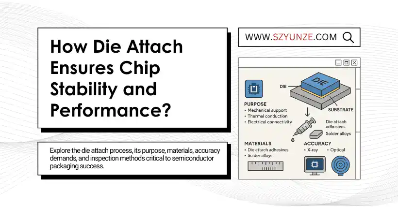
Purpose and Technical Requirements of Die Attach
✅ Core Purposes:
- Fix chip position: Ensure the chip doesn’t move or tilt during the packaging process.
- Thermal and electrical conduction: Some die attach materials also serve as thermal and electrical paths (especially for power devices).
- Withstand thermal and mechanical stress: The attachment method must accommodate thermal expansion and cooling during subsequent steps, preventing chip cracking or detachment.
⚙️ Technical Requirements:
- High precision in placement (especially for large or multi-chip packages; error must be within ±50μm).
- Uniform adhesive or solder layer thickness to avoid voids or bubbles.
- Adequate contact area under the chip to aid heat dissipation and mechanical stability.
- For ultra-thin chips, suction force must be controlled to prevent cracking or microfractures.
03
Common Die Attach Methods (by Material Type)
- Silver Epoxy Adhesive
One of the most common methods:
- Uses conductive epoxy with silver particles to attach the chip to the leadframe.
- Silver improves thermal and electrical conductivity.
- Adhesive thickness is typically around 5μm.
- Process requires visible silver epoxy overflow around ≥90% of the chip edges to ensure solid bonding and good heat conduction.
- Application: Suitable for most standard package types.
- Eutectic Bonding
Uses eutectic materials like gold-silicon (Au-Si) that melt upon heating to form metallic bonds.
- Melting point is around 370°C; temperature and time must be precisely controlled.
- Offers high reliability, electrical, and thermal performance.
- Application: Commonly used for high-power, high-reliability chips such as RF and automotive devices.
- Solder Attach
Uses solder wire or solder paste melted by heat for die attachment.
- Process temperature is slightly lower than eutectic bonding (e.g., SnAgCu alloy melts at ~220°C).
- Faster speed; suitable for small chip sizes.
- Application: Ideal for high-volume, cost-sensitive products.
04
Key Process Control Points in Die Attach
| Control Item | Key Requirement |
|---|---|
| Adhesive or solder amount | Precisely controlled to prevent overflow or weak bonding |
| Chip placement accuracy | High accuracy needed for large chips (≤50μm error) |
| Bonding pressure and time | Excess may damage chip; too little may cause weak adhesion |
| Temperature control | Critical during curing or soldering; precise regulation needed |
| Epoxy overflow check | ≥90% chip edge should show visible silver epoxy overflow |
05
Special Considerations in Die Attach
For large chips:
- Larger size requires higher placement accuracy.
- More susceptible to thermal expansion/contraction; stress distribution in adhesive or solder layer must be optimized.
For ultra-thin chips:
- Extremely fragile and prone to cracking or microfractures.
- Die bonder must use soft tips or vacuum pads with cushioning and reduced movement speed.
06
Post Die Attach Inspection Methods
After die attach, typical inspections include:
- X-ray inspection: To detect voids, bubbles, or misalignment.
- Cross-sectional SEM analysis: To verify adhesive layer thickness and overflow status.
- Optical microscope inspection: To confirm silver epoxy overflow and chip centering.
- Thermal resistance testing (especially for power devices): To assess thermal conduction performance.
07
Summary
Die attach is a crucial bridge between the chip and the package substrate, forming the basis for the entire packaging process. It not only determines whether the chip is securely fixed but also affects the device’s thermal, electrical, and mechanical performance and reliability.
In short: Die attach is not just “gluing the chip,” but a precise engineering process involving bonding materials, thermodynamics, electrical contact, and stress management.
Related:

Disclaimer: This article is created by the original author. The content of the article represents their personal opinions. Our reposting is only for sharing and discussion purposes and does not imply our endorsement or agreement. If you have any objections, please get in touch with us through the provided channels.