
In the continuous evolution of semiconductor manufacturing, the development of advanced processes has always been the key driving force for industry progress. When the process technology advances to 28 nanometers and below, HKMG (High-K Metal Gate) technology has become an indispensable presence.
From a physical principle perspective, as the process size shrinks, traditional materials and technologies face severe challenges. In transistors, the gate, as the key structure controlling current, directly affects the overall performance of the chip. When the process reaches below 28 nanometers, if traditional silicon dioxide (SiO₂) is still used as the gate dielectric, its relatively low dielectric constant (about 3.9-4.5) will require the gate oxide thickness to be constantly reduced to maintain effective control over the channel. However, when the gate oxide thickness drops below 2 nanometers, severe quantum tunneling effects occur, leading to a sharp increase in leakage current, significantly raising the chip’s power consumption, and drastically reducing performance.
Here, the concept of EOT (equivalent oxide thickness) needs to be introduced. EOT is defined as the thickness of the gate dielectric material that gives the same gate capacitance as pure SiO₂.
According to the above formula and the concept of EOT, we can understand that under the premise of keeping the high-k material thickness (Thigh-k) constant, since the dielectric constant of high-k materials is greater than that of SiO₂/SiON, the EOT is smaller, allowing the transistor size to continue shrinking according to Moore’s Law.
High dielectric constant (High-K) materials in HKMG technology, such as hafnium oxide (HfO₂, with a dielectric constant of 20-25 or even higher), can achieve stronger electric field control at the same physical thickness, greatly reducing leakage current. For example, by replacing SiO₂ with HfO₂, at the same electric field strength, the thickness of the gate dielectric can be increased several times, effectively suppressing the quantum tunneling phenomenon, thereby enhancing transistor performance and stability.
In addition to the high k-value, the dielectric material must also consider factors such as material barriers, energy gaps, interface state density and defects, chemical and thermal stability, and compatibility with standard CMOS processes. HfO₂-based high-k dielectrics are currently one of the most promising choices (followed by ZrO₂-based high-k dielectrics).
The dielectric constant, denoted by ε, is measured in Farads per meter (F/m), and reflects the efficiency of a dielectric material in binding charges. The larger the value, the more firmly the charges are bound within the material, increasing its insulating properties. Under the same external electric field, materials with a larger dielectric constant exhibit lower charge polarization, producing relatively smaller polarized charges and electric fields.
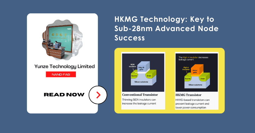
However, when traditional polysilicon gates are paired with high dielectric constant materials, problems such as threshold voltage drift arise, severely affecting the consistency and stability of transistor performance. This is because polysilicon can react with hafnium (Hf) in the high-k dielectric HfO₂, creating interface defects. Additionally, the higher resistivity of polysilicon increases gate resistance, which leads to a higher RC delay and thus reduces circuit speed. Eliminating the Poly-Depletion Effect, when the polysilicon layer near the gate dielectric is depleted during the “on” state, reduces the effective capacitance of the gate. In contrast, metal gates are excellent conductors, and no depletion region occurs in the gate material.
The metal gate in HKMG technology effectively solves this problem. Metal gates, typically made of titanium, tantalum, and other metal alloys, have better work function matching with semiconductor materials and can precisely adjust the threshold voltage of transistors, avoiding threshold voltage drift. At the same time, metal gates have lower resistance than polysilicon gates, resulting in lower energy loss during current transmission through the gate, further reducing chip power consumption and improving transistor switching speed.
As process nodes continue to shrink, the performance requirements for transistors become increasingly stringent. HKMG technology enables the reduction of device size while maintaining or even improving transistor performance, meeting the demand for high-performance chips in advanced processes. In 28-nanometer and below processes, HKMG technology allows transistors to maintain size reduction while reducing leakage current to below one-tenth of that in traditional processes, greatly enhancing chip integration and performance. This performance improvement is reflected not only in computation speed but also in the accuracy and stability of data processing, providing strong support for fields that require extremely high chip performance, such as high-performance computing, artificial intelligence, and 5G communications.
Although HKMG technology has irreplaceable advantages in advanced processes below 28 nanometers, it also faces challenges such as high process complexity and increased costs. HKMG processes require near-precise equipment accuracy, material purity, and process monitoring, leading to a 30% or higher increase in production line investment compared to traditional processes. However, with continuous technological development and maturity, these issues are gradually being resolved. It is believed that in the future, HKMG technology will continue to play a key role in advanced processes and drive the continuous development of the semiconductor industry.
Related:
- What Is Cgd Capacitance in a MOSFET Explained
- Metal ECP: How Much Edge Cleaning is Needed?
- Memory Cell Wear: NAND Cycles vs DRAM Aging

Disclaimer:
- This channel does not make any representations or warranties regarding the availability, accuracy, timeliness, effectiveness, or completeness of any information posted. It hereby disclaims any liability or consequences arising from the use of the information.
- This channel is non-commercial and non-profit. The re-posted content does not signify endorsement of its views or responsibility for its authenticity. It does not intend to constitute any other guidance. This channel is not liable for any inaccuracies or errors in the re-posted or published information, directly or indirectly.
- Some data, materials, text, images, etc., used in this channel are sourced from the internet, and all reposts are duly credited to their sources. If you discover any work that infringes on your intellectual property rights or personal legal interests, please contact us, and we will promptly modify or remove it.