

On October 11, 2023, Micron Corporation announced the further expansion of its 1β process node technology, introducing 16GB DDR5 memory.

Micron has begun offering its 1β DDR5 DRAM, which can achieve peak speeds of up to 7200 MT/s, to data center and PC users. This new DDR5 memory utilizes advanced high-k CMOS device technology, and features 4-phase clocking, and clock synchronization. Compared to the previous generation, it offers a 50% increase in performance and a 33% improvement in performance per watt.
The new 1β DDR5 DRAM product line provides module densities ranging from 4,800 MT/s to 7,200 MT/s, catering to the demands of data centers and client applications.
Brian Callaway, Vice President of Micron’s Core Compute Design Engineering Group, emphasized the significance of this development, stating, “The mass production and availability of 1β DDR5 DRAM for client and data center platforms mark a significant milestone in the industry. Our collaboration with ecosystem partners and customers will drive faster adoption of these high-performance memory products.”
Micron’s 1β technology supports a variety of memory-based solution combinations, including DDR5 RDIMM and MCRDIMM using 16Gb, 24Gb, and 32Gb DRAM chips, as well as LPDDR5X, HBM3E, and GDDR7 using 16Gb and 24Gb DRAM chips. The 16Gb DDR5 memory products will be sold through direct sales and channel partners.
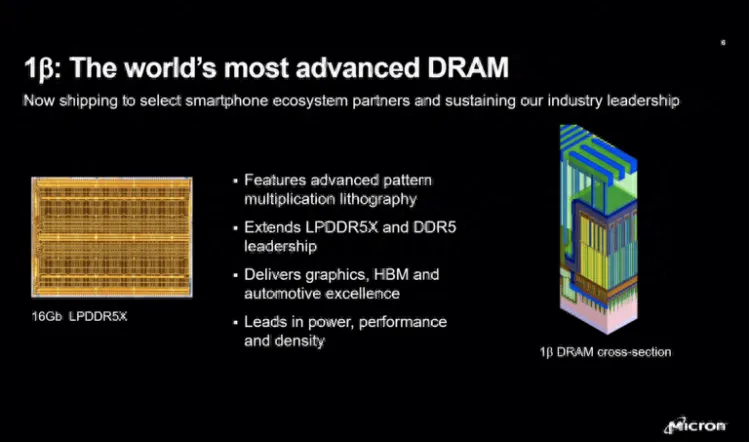
In November of last year, Micron officially introduced its 1β node DRAM products and has already conducted sample testing with smartphone and chip platform partners. According to Micron, the 1β node DRAM products are ready for mass production and will be first adopted in LPDDR5X mobile memory, achieving speeds of up to 8.5Gb/s.
It’s worth noting that industry analysis firm TechInsights found that the iPhone 15 Pro uses Micron’s latest ultra-low-power D1β (D1b) LPDDR5 16Gb DRAM chip internally, marking Micron’s entry into D1β technology for the first time.
As the world’s most advanced DRAM process node, 1β represents progress in the company’s market leadership. The shipment volume of 1α (1-alpha) in 2021 solidified this position. Compared to 1α, 1β technology improves energy efficiency by about 15%, increases bit density by over 35%, and has a chip capacity of 16Gb.
Reportedly, compared to 1α, 1β technology can improve energy efficiency by about 15%, increase memory density by over 35%, and have a single bare die capacity of up to 16Gb. Micron believes that with the introduction of LPDDR5X, the mobile ecosystem will be the first to benefit from the advantages of 1β DRAM products, unlocking the next generation of mobile innovation and advanced smartphone experiences while reducing power consumption.
It’s evident that both the MediaTek Dimensity 9200 processor and the Qualcomm Snapdragon 8Gen2 mobile platform now include support for LPDDR5x memory, making it a standard feature for the new generation of flagship smartphone processors. Smartphone manufacturers have already begun extensive verification and usage of LPDDR5x, signaling a significant iteration from LPDDR5 to LPDDR5x in smartphone products. This will bring performance enhancements to mobile, gaming, camera, and artificial intelligence applications, along with more new features, ultimately enhancing the user experience.
01
Micron, by tackling the challenges of complex photolithography and nanomanufacturing, has defied the laws of physics.
The leading-edge 1β node from Micron can achieve higher memory capacities within a smaller footprint, ultimately reducing the cost per unit of data. The scalability of DRAM is heavily reliant on the ability to integrate more and faster memory on each square millimeter of semiconductor wafer area. This necessitates shrinking circuitry dimensions to accommodate billions of memory cells on a chip the size of a fingernail. Over the past few decades, as process nodes have continued to advance, the semiconductor industry has regularly reduced device sizes each year or every two years. However, as chips have become smaller, defining circuit patterns on wafers has begun to challenge the laws of physics.
To overcome these technological challenges, the semiconductor industry has started using new equipment with extreme ultraviolet photolithography technology. However, this technology is still in its early stages. To mitigate technological risks, Micron has leveraged its mature state-of-the-art nanomanufacturing and photolithography technology. Using proprietary advanced multiple exposure and immersion photolithography technologies, the company forms patterns with the utmost precision on a small scale. Shrinking device sizes to provide larger capacity will enable smaller form factor devices like smartphones and IoT devices to integrate greater memory within compact spaces.
To achieve a competitive edge in both 1β and 1α technologies, Micron has actively advanced its manufacturing, engineering capabilities, and groundbreaking research and development over the past few years. This accelerated innovation initially positioned Micron’s 1α node ahead of the competition by a year, establishing Micron’s leadership in the DRAM and NAND fields for the first time in company history. Over the past three years, Micron has further invested billions of dollars to transform its wafer fabs into leading-edge, highly automated, sustainable, and AI-driven facilities. This includes investments in Micron’s factory in Hiroshima, Japan, which will be used for mass production of DRAM on the 1β node.
02
The 1β node from Micron lays a solid foundation for an interconnected and sustainable world.
With the rise of energy-intensive use cases like machine-to-machine communication, artificial intelligence, and machine learning, the demand for energy-efficient technologies is becoming increasingly urgent for businesses, particularly those aiming to achieve stringent sustainability goals and reduce operational costs. Researchers have found that training an artificial intelligence model can emit carbon emissions over its entire lifecycle five times greater than that of a U.S. car, including its manufacturing. Furthermore, it is expected that by 2030, information and communication technology will consume 20% of the world’s electricity.
Micron’s 1β DRAM node provides a versatile foundation for progress in the interconnected world. This world requires fast, ubiquitous, and energy-efficient memory to drive digitization, optimization, and automation. High-density, low-power storage manufactured on the 1β node can facilitate more energy-efficient data flows among data-intensive smart devices, systems, and applications, as well as greater intelligence from the edge to the cloud. In the coming year, the company will begin introducing the rest of its 1β product portfolio in embedded, data center, client, consumer, industrial, and automotive sectors, including graphics memory and high-bandwidth memory, among others.
Recommended:
- Understanding Mobile Phone RAM: What You Need to Know
- Micron Resolves Dispute with Fujian JHICC: Industry Impact

Disclaimer: This article is created by the original author. The content of the article represents their personal opinions. Our reposting is for sharing and discussion purposes only and does not imply our endorsement or agreement. If you have any objections, please contact us through the provided channels.