
The global adoption rate and production capacity of packaging design are continuously expanding. Packaging capacity is one aspect, while on the other hand, there is a growing demand for testing and evaluation before investing resources into prototype substrates and packaging. This means that designers need to use simulation tools to comprehensively assess packaging substrates and interconnections.
The packaging of heterogeneous integrated devices is a very advanced design, which naturally requires electrical simulation. But do these thermo-mechanical systems need other simulations as well? As you may have guessed, ensuring high-reliability packaging involves a series of tests, and multi-purpose simulation tools can provide highly accurate results.
01
Three Simulation Areas in Advanced Packaging
In broad terms, simulations and experiments need to be conducted in three different areas to ensure reliability. Simulation should be carried out first, as it provides the design team with the opportunity to modify the packaging before testing. The three main simulation areas are: electrical, mechanical, and thermal.
The following diagram shows typical 3D simulation results of a simple chip package and its lead frame. Although only the thermal results are shown in the diagram, in principle, thermal behavior is associated with both electrical and mechanical behaviors, depending on the packaging material properties. When validating reliability, it is necessary to combine specialized simulation software to examine these three areas.
02
Thermal-Mechanical Simulation
Both thermal and mechanical simulations are important, but from the perspective of ensuring reliability, thermal-mechanical multiphysics simulation is equally crucial. These simulations can enter the nonlinear domain, presenting scenarios in extreme temperature changes or repetitive thermal cycles.
When considering both thermal and mechanical behaviors in the same system, we can observe thermal stresses in the packaging, allowing for a more accurate assessment of reliability. Multiphysics simulation requires well-defined material parameters as input to achieve accurate results. Through simulation, multiple performance aspects can be assessed, such as fatigue, stress and strain, as well as interface stresses caused by mismatched thermal expansion coefficients.
| Only Thermal Simulation | ✅ Under the known average current consumption, the steady-state temperature should be determined |
| Only Mechanical Simulation | ✅ Mechanical impact response ✅ Response to repeated impacts ✅ Vibration within the package |
| Thermal-Mechanical Simulation | ✅ Thermal expansion will generate stress in various areas of the package |
03
Electrical Simulation
Advanced packaging of heterogeneous integrated devices leads in terms of electrical performance, typically operating at relatively more advanced technology nodes. This often means very high data rates, very small interconnect structures, high channel bandwidth requirements, and the need for unique wiring methods, such as cross-layer routing.
When looking inside the package, we can see that validation in several areas requires full-wave electromagnetic simulation. First, signal integrity simulation is necessary:
| Vertical Transition to PCB | ✅ The through hole and its passage through the internal plane (if present) need to have matching impedance and maintain TEM mode propagation. ✅ Ball-out usually sets limitations on the TEM propagation mode in the package. |
| Substrate Shannel Wiring | ✅ The channel must have low crosstalk ✅ The channel must maintain TEM mode propagation |
| Crosstalk Between Channels | ✅ The array of vias in the encapsulation wiring sets the shielding effect between channels |
| Bump and RDL Interface | ✅ When there is impedance mismatch, Bump-out and RDL wiring may cause excessive return loss in the channel |
| Vertical Transition between Bare Chips | ✅ In packaging, the vertical transition between bare chips is formed by vias or TSVs. ✅ These transitions are high-speed channels, but they also need to be checked in thermal-mechanical simulations. |
For simpler interfaces that connect to the PCB, high-speed signal integrity simulation is not as critical. However, if the package supports advanced devices with the latest high-speed interfaces, electrical simulation becomes very important. The signal must not be lost before reaching the ball-out at the bottom of the package, and the above simulation list aims to determine when this occurs.
An important area for simulation in the package is power distribution. Power integrity and power distribution topology in the package are as important as in the PCB. In fact, these two areas work together to ensure low impedance across a very wide bandwidth. Power in the package is mainly supplied by power rails and ultimately transmitted to the die bump through RDL routing. The system must provide low impedance in the higher frequency range where the PCB becomes inductive.
| Power Supply Stability | ✅ Based on packaging parasitic effects and substrate structure, the power supply rail ripple should be predictable. |
| Current Consumption | ✅ To predict the packaging working temperature, it is necessary to understand the total current consumption and determine the thermal resistance. ✅ Once the current consumption is mastered, the quality of the packaging material can be determined. |
| Bare Chip Capacitors | ✅ Bare chip capacitors and packaged chip capacitors can provide low PDN impedance in the GHz range and at higher frequencies. |
| Packaging Capacitors and Inductors | ✅ The packaging capacitor is provided by the power rail in the substrate and the intermediate layer. ✅ The vertical track transition and bump have a certain inductance, which will increase the PDN impedance. |
The latest simulation mode in this field balances the effects of power on signal integrity, where power failures and power integrity are also considered as part of the signal integrity simulation process. These simulation methods are unconventional and require the use of very complex SPICE circuits to predict both power and signal behaviors within the same simulation. The Cadence Celsius Thermal Solver is the first thermal analysis technology specifically designed for electrical and mechanical engineers. Electrical engineers can extend power integrity analysis with fast, accurate, and easy-to-use thermal simulations, while mechanical engineers can extend their existing thermal analysis methods to include real thermal sources generated by electro-thermal interactions.
Related:
- Why GPU Chips Now Rely on Embedded Liquid Cooling
- Why ESC Surface Treatment Drives Real Performance?
- Improve PCB Cooling Easily with Smart Design Ideas
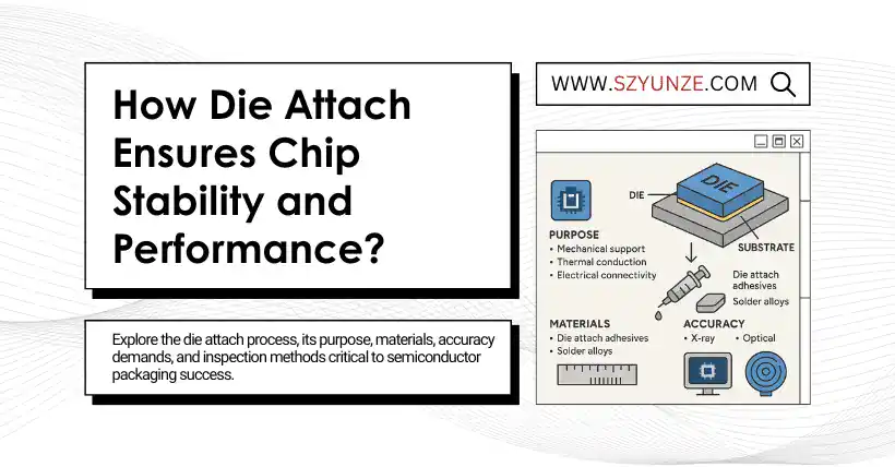
- How Die Attach Ensures Chip Stability and Performance?
- Top Software Tools Used in Chip Front End Design

Disclaimer:
- This channel does not make any representations or warranties regarding the availability, accuracy, timeliness, effectiveness, or completeness of any information posted. It hereby disclaims any liability or consequences arising from the use of the information.
- This channel is non-commercial and non-profit. The re-posted content does not signify endorsement of its views or responsibility for its authenticity. It does not intend to constitute any other guidance. This channel is not liable for any inaccuracies or errors in the re-posted or published information, directly or indirectly.
- Some data, materials, text, images, etc., used in this channel are sourced from the internet, and all reposts are duly credited to their sources. If you discover any work that infringes on your intellectual property rights or personal legal interests, please contact us, and we will promptly modify or remove it.