
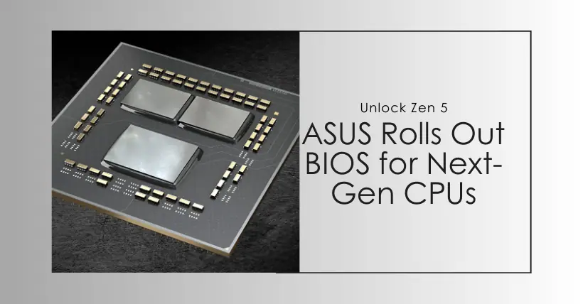
This year, AMD is definitely going to launch a new generation of Zen 5 architecture processors, possibly the Ryzen 9000 series, especially since the 8000 series has already been taken by mobile APUs. The codename for the desktop version of the Zen 5 processor is Granite Ridge, and it will continue to use the AM5 platform. Therefore, users who have already purchased the X670 and B650 motherboards won’t need to replace their motherboards and DDR5 memory to support AMD’s next-generation processor. Of course, the motherboard will definitely need a BIOS update at that time.
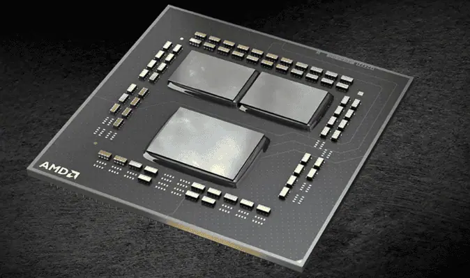
However, logically speaking, there’s still a long time before Zen 5 is officially released, so motherboard manufacturers shouldn’t start preparing so early. But today, ASUS updated the BIOS on its X670E motherboard, upgrading the AMD microcode to AGESA 1.1.7.0. This new BIOS has two features: one is support for 256GB of memory capacity, and the other is support for the Zen 5 processor, codenamed Granite Ridge.
It’s somewhat strange for ASUS to make its motherboards support the next generation of AMD processors so early. We speculate that AMD has already sent a test version of the Zen 5 processor to manufacturers, which is why ASUS updated the motherboard BIOS to test compatibility. Previously, Granite Ridge’s ES was found on AMD’s shipping list, one being a 170W B0 step 8-core, and the other a 105W A0 step 6-core, indicating that AMD has provided motherboard manufacturers with early samples of the Zen 5 architecture processor for debugging the new BIOS. So, in addition to ASUS, other manufacturers like MSI and Gigabyte are likely to update their BIOS soon.
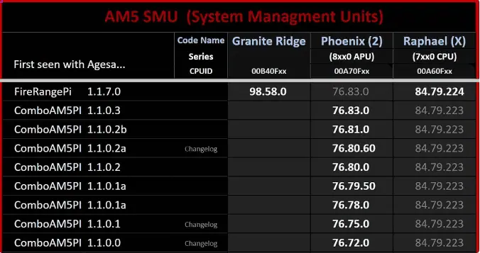
Moreover, according to ASUS’s release page, AMD seems to have changed the naming of its microcode. The previous BIOS microcode name for AMD was ComboAM5PI, and now it’s changed to FireRangePi. Interestingly, FireRange is actually the codename for the mobile version of Zen 5, which suggests that AMD is quite meticulous with its naming. From what we can see, the earliest Zen 5 might officially debut at the Taipei Computer Exhibition in June. So even if the motherboard updates the BIOS, consumers don’t have a product to use yet, unless someone can buy AMD’s test processor.
As for when Zen 5 will be on the market, we estimate it to be around the third quarter, similar to the previous generation Zen 4. This means consumers can expect benefits during China’s Double Eleven sales, as AMD’s price reductions are significant. If you’re not eager for the first release, it’s better to wait for a while before purchasing to get a good discount. And if you’re more patient, perhaps current Zen 4 processor users should wait until the Zen 5 X3D version is released before considering an upgrade.

Regarding the Zen 5 processor, we only know from rumors that its performance is expected to increase by 40% compared to the previous generation, though it’s unclear if this refers to IPC or multi-core performance. Regardless, AMD is sure to bring us exceptionally performing products. From our perspective, AMD might also incorporate an NPU module in Zen 5 to meet the needs of AI PCs. Anyway, we’ll get more information in the latter half of this year and can only hope that AMD doesn’t set the price too high.
Bonus: AMD Zen 5 execution engine exposed: Uses a true 512-bit FPU
The news source Moore’s Law is Dead shared information about the AMD Zen 5 processor Execution Engine in the latest video, stating that it will use a true 512-bit Floating Point Unit (FPU).
According to the slides shared by the source, the Execution Engine of Zen 5 is described in detail, utilizing a true 512-bit FPU.
The AMD Zen 4 processor uses a dual 256-bit FPU when executing AVX-512 instruction workloads, while Zen 5 uses a true 512-bit FPU, which will perform better in processing 512-bit AVX or VNNI instructions.
The editor also learned from the report that AMD upgraded related components for the 512-bit FPU, increased the capacity of L1 DTLB, expanded the load-store queue, doubled the bandwidth of the L1 data cache, and increased its size by 50%. The size of L1D has increased from 32 KB in “Zen 4” to 48 KB now.
The FPU MADD latency has been reduced by one cycle. Besides the FPU, AMD also increased the number of integer execution pipes from 8 (Zen 4) to 10, and the size of the exclusive level 2 cache per core remains at 1 MB.
Related:
- The 2025 Chip Showdown: Top Four Markets at Stake
- Key AMD GPU Leader Steps Down: What’s Next?
- Why NVIDIA Leads Over AMD: Key Factors Explained

Disclaimer: This article is created by the original author. The content of the article represents their personal opinions. Our reposting is for sharing and discussion purposes only and does not imply our endorsement or agreement. If you have any objections, please contact us through the provided channels.