
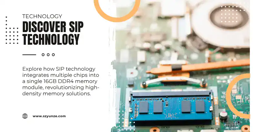
With the advancement of DDR technology, 16GB DDR4 memory modules are now commonplace, but have you ever seen a 16GB DDR4 chip? Currently, the mainstream single-chip capacity is 1GB or 2GB, so how is a 16GB DDR4 chip achieved? Today, let’s talk about the SIP technology that makes a single 16GB chip possible.
SIP, short for System in Package, refers to a high-density integration technology that integrates multiple active chips, passive components, MEMS devices, optical components, etc., into a single package to perform certain system functions. Based on existing mature chips, different functional bare chips are integrated onto a single package substrate, forming a small system. Compared to SoC (System on Chip), the design becomes more flexible, with shorter development cycles, lower development costs, and relatively higher yields.
By stacking nine 16Gb bare die on a package substrate, the limitations of two-dimensional space are overcome, significantly improving the integration density per unit area, effectively putting a memory module into a single chip package. This is how a 16GB DDR4 chip is born. Want to know how the dies are stacked in the package? Hold on tight, here’s a high-energy warning!
The internal bonding technology of SIP can use pure wire bonding (WireBond), flip-chip bonding (FlipChip), or a combination of both. Additionally, there is also a silicon via (Through-Silicon Via, TSV) connection method.
FlipChip: This involves depositing tin-lead balls on the I/O pads, then flipping the chip and heating it to combine the molten tin-lead balls with the substrate. This packaging method is also called “inverted bonding.” FlipChip offers superior electrical and thermal performance, as well as higher I/O pins. Therefore, dies with many I/O pads, such as FPGAs, typically use FlipChip as the bonding method.
WireBond: This refers to connecting the die to the package substrate using wires. It has mature technology, low production costs, and flexible design. It allows the die to break through the area limitations of the package substrate, enabling multi-layer stacking of chips.
SIP not only allows for ultra-high capacity DDR chips but also enables system integration of high-speed chips. However, due to the inductive nature of bonding wires, which act as impedance-discontinuous lines, the bonding wire performance in conventional designs may not meet the needs of high-speed signal transmission. To address this, we can accurately model and simulate gold wire performance to assess and optimize it for high-speed transmission. We can also conduct passive and active simulations of the entire PCB+Package link.
At the same time, power and GND are also connected through bonding wires, so the impact of bonding wires on DC voltage drop and PND impedance needs to be considered. Package-level power simulations can evaluate voltage drops and noise, providing optimization plans to meet power performance requirements. PCB+Package+die combined simulations can be used to simulate the system-level power performance.
The stacking methods of different dies mentioned above are all from SIP design simulation examples. Additionally, different bonding methods and die specifications can also be stacked. Specific evaluation is required based on the type of die, size, pin distribution, bonding method, packaging layers, and other factors. Due to space limitations, we won’t list them all here, but if you are interested, I will share some SIP examples with you later.
Related:

Disclaimer:
- This channel does not make any representations or warranties regarding the availability, accuracy, timeliness, effectiveness, or completeness of any information posted. It hereby disclaims any liability or consequences arising from the use of the information.
- This channel is non-commercial and non-profit. The re-posted content does not signify endorsement of its views or responsibility for its authenticity. It does not intend to constitute any other guidance. This channel is not liable for any inaccuracies or errors in the re-posted or published information, directly or indirectly.
- Some data, materials, text, images, etc., used in this channel are sourced from the internet, and all reposts are duly credited to their sources. If you discover any work that infringes on your intellectual property rights or personal legal interests, please contact us, and we will promptly modify or remove it.