
Many people might assume that the higher the PCB signal rate—such as 25Gbps or 56G/112G-PAM4 signals—the more debugging issues you’ll encounter. In reality, that’s not the case. The most frequent debugging issues we receive actually involve DDR3 and DDR4. Common problems include failing to reach the rated speed, the system failing to recognize the memory, or errors occurring during the training process. In these situations, engineers often spend a long time debugging without finding the root cause, eventually suspecting the PCB design—since the hardware schematics and software are usually provided by the manufacturer and are considered the “least likely to be wrong.”
The reason debugging is so troublesome, especially after an issue arises, is that there are too many factors involved. As the saying goes, “to each their own specialty”; we can only troubleshoot from the perspective of PCB design, signal integrity (SI), or power integrity (PI). If the issue lies within the hardware logic or software, we might be at a total loss. Using today’s case study, we can briefly discuss how to generally handle these DDRx issues during the debugging process.
01
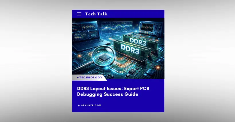
Case Background of DDR3 Layout Issues
A customer discovered during debugging that their DDR3 could only function normally with a single chip at a low frequency. Multiple chips could not operate together correctly. After debugging for a long time without success, they reached out to us to review the PCB design or perform physical signal testing.
Test Results:
- At 400MHz Clock (800Mbps Data Rate):
- Board 1: Only Channel A, Chip 0 (the first chip next to the main SoC) passed. All other chips failed with errors.
- Board 2: Only Channel A, Chips 0, 1, and 3 passed. All others failed.
- At 800MHz Clock (1600Mbps Data Rate):
- All chips on all boards failed with errors.
According to our usual experience: if DDRx cannot run at its rated speed but improves when the frequency is lowered, it typically indicates a timing margin issue. This is usually related to the PCB design or the configuration of Drive Strength and ODT (On-Die Termination). There is a high probability of finding and solving these problems through board reviews or simulations.
Since this specific problem showed improvement at lower frequencies, we asked the customer for their PCB design files—our standard troubleshooting procedure.
02
Identifying the Flaws
Upon reviewing the PCB layout, we found several issues. Here are the most prominent ones:
- Pin Delay Ignored: When calculating trace length matching (equalization), the chip’s internal pin delays were not included, which negatively impacts timing.
- Incomplete Length Matching Rules: Address line rules were only set for the “main trunk” (from the SoC to the first chip). The “branches” between subsequent chips had no rules, further affecting timing.
- Incorrect Termination Placement: The clock used a Fly-by topology, but the termination resistors were placed near the first chip instead of the last chip. This is a critical error.
03
The Solution
Experienced engineers will likely spot the fatal flaw immediately (Point 3). We instructed the customer to perform a quick experiment: move the resistors (circled in red in the layout) and solder them to the P/N pins corresponding to the last chip in the chain.
Because Channel B suffered from the same issue (and performed even worse), we had them move the clock network resistors for that channel as well.
04
The Result
The next day, we received good news: after moving the resistors as suggested, the problem was solved.
This case demonstrates that while a board review may reveal many details that don’t meet standard PCB design requirements, the key is identifying which specific flaw is the “fatal” one. It also shows that at relatively lower speeds, even if you ignore factors like pin delay, the system might still function—though these factors do eat away at your timing margin. Our job is to claw back as much of that margin as possible from every angle.

Disclaimer:
- This channel does not make any representations or warranties regarding the availability, accuracy, timeliness, effectiveness, or completeness of any information posted. It hereby disclaims any liability or consequences arising from the use of the information.
- This channel is non-commercial and non-profit. The re-posted content does not signify endorsement of its views or responsibility for its authenticity. It does not intend to constitute any other guidance. This channel is not liable for any inaccuracies or errors in the re-posted or published information, directly or indirectly.
- Some data, materials, text, images, etc., used in this channel are sourced from the internet, and all reposts are duly credited to their sources. If you discover any work that infringes on your intellectual property rights or personal legal interests, please contact us, and we will promptly modify or remove it.