
Semiconductor manufacturing is a typical “precision-first” field, especially in the front-end wafer processing and back-end packaging stages, where grinding and polishing technologies directly determine the performance and yield of devices. The following analysis is based on three aspects: technical principles, process challenges, and industry trends.
1. Grinding Technology: Wafer Thinning and Surface Planarization
Principle: Grinding achieves precise material removal through mechanical abrasion and chemical synergistic effects. Traditional grinding relies on mechanical cutting with superhard abrasives such as diamond, while new processes combine chemical etching (e.g., mechanical-chemical polishing) to reduce surface damage and improve efficiency.
✅ Technical Challenges of Grinding Technology
Stress Control: Mechanical grinding can introduce micro-cracks and residual stresses, which require optimization of abrasive size, pressure, and coolant flow to minimize damage.
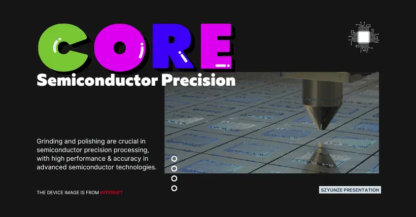
Uniformity: Grinding large 300mm wafers must ensure that the thickness variation across the wafer is less than ±1μm. The increase in substrate size makes it difficult to control grinding uniformity.
✅ Trends of Grinding Technology
Ultra-Thin Wafer Processing: For 3D packaging requirements, thinning to below 20μm requires the integration of temporary bonding/debonding technologies.
Composite Processes: Combining mechanical grinding with wet etching to improve efficiency and reduce defects.
2. Polishing Technology: Atomic-Level Surface Finishing
Chemical Mechanical Polishing (CMP): Semiconductor polishing mainly uses CMP, which achieves atomic-level surface flatness (roughness < 0.1nm) through the synergistic effects of chemical etching and mechanical grinding.
✅ Key Elements of Polishing Technology
Polishing Slurry: Chemical agents containing nano-sized SiO₂ or CeO₂ particles, with customized formulas based on the material (Si, SiO₂, Cu, etc.).
Polishing Pad: Porous polyurethane material, which requires regular conditioning to maintain surface morphology consistency.
✅ Challenges Polishing Technology
Material Selectivity: Controlling the synchronized polishing rate of different materials (e.g., Cu and dielectric layers) in multilayer structures.
Defect Control: Detection and suppression of micro-scratches and residual particles (requires in-situ cleaning and megasonic assistance).
✅ Emerging Technologies of Polishing Technology
Electrochemical Polishing (ECMP): Stress-free polishing for copper interconnects, reducing dishing.
Plasma Polishing: Non-contact high-precision processing for wide bandgap materials such as diamond, GaN, and SiC.
3. Industry Technical Challenges and Future Directions
✅ Processing Bottlenecks for Third-Generation Semiconductors
High-hardness materials like diamond, SiC, and GaN place higher demands on grinding and polishing equipment (e.g., the grinding efficiency of SiC wafers is only 1/10th that of silicon), driving the development of composite processes such as laser-assisted processing and plasma etching.
✅ Demand for Large-Size and High Integration
450mm wafers and GAA transistor structures require global polishing flatness to within 0.5nm, driving the upgrade of multi-zone pressure-adjusting polishing heads and intelligent online monitoring systems.
✅ Green Manufacturing and Cost Control
Polishing slurry recovery and low-consumption processes (e.g., fixed abrasive polishing pads) have become industry focal points, while AI-driven process parameter optimization can reduce energy consumption by more than 20%.
Related:

Disclaimer:
- This channel does not make any representations or warranties regarding the availability, accuracy, timeliness, effectiveness, or completeness of any information posted. It hereby disclaims any liability or consequences arising from the use of the information.
- This channel is non-commercial and non-profit. The re-posted content does not signify endorsement of its views or responsibility for its authenticity. It does not intend to constitute any other guidance. This channel is not liable for any inaccuracies or errors in the re-posted or published information, directly or indirectly.
- Some data, materials, text, images, etc., used in this channel are sourced from the internet, and all reposts are duly credited to their sources. If you discover any work that infringes on your intellectual property rights or personal legal interests, please contact us, and we will promptly modify or remove it.