
Let’s talk about the semiconductor industry chain today.
In today’s era of ubiquitous connectivity, few industries are as fundamental as semiconductors. No other field has such tightly interwoven technical links, where a single point of failure can impact the whole system. Chips are no longer just a buzzword in the tech world—they are closely tied to a nation’s industrial security, technological independence, and future competitiveness.
From materials and equipment to design and manufacturing, from packaging and testing to downstream applications, the semiconductor industry has formed a complex and precise industrial chain. This is a sector with extremely high entry barriers, intense technological demands, heavy capital investment, and long development cycles—which also makes it one of the most strategically valuable tracks in the global arena.
The starting point of semiconductors is not chip design, but the most basic materials and equipment.
Whether it’s a high-performance CPU or an AI accelerator, it all begins with a small silicon wafer. Key materials like wafers, photoresists, specialty electronic gases, and sputtering targets form the cornerstone of chip manufacturing. A failure in any of these areas would make it impossible to proceed with advanced processes.
The lithography machine—often called the “crown jewel of industrial manufacturing”—is the most iconic equipment in the semiconductor ecosystem. Beyond ASML’s EUV lithography machines, etching machines, deposition tools, and cleaning equipment are all indispensable high-tech instruments. Their precision directly determines how advanced and efficient chip production can become.
EDA (Electronic Design Automation) software is the arsenal of chip designers. Without EDA, designing chips would be like groping in the dark. From circuit layout and timing analysis to verification and simulation, none of it is possible without these tools. The global EDA market is highly concentrated, dominated by three giants: Synopsys, Cadence, and Mentor.
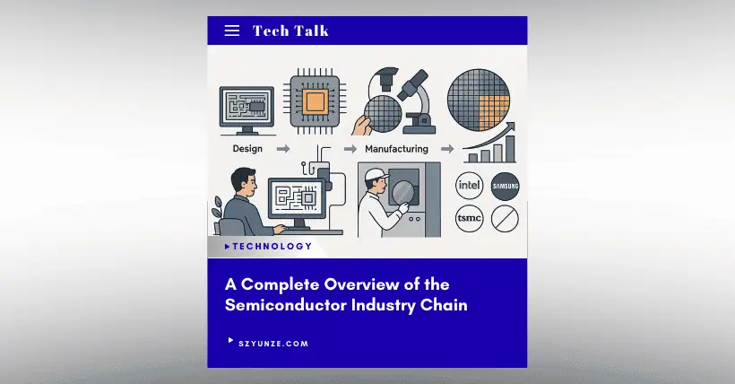
The midstream segment serves as the “central nervous system” of the semiconductor industry chain, mainly comprising three key areas: IC design, wafer manufacturing, and packaging and testing.
- IC Design: This is where ideas are turned into blueprints. Design companies, based on customer needs and product positioning, use EDA tools to plan circuits and build chip architectures. China has made rapid strides in this area in recent years, with rising stars like Huawei HiSilicon, Cambricon, Will Semiconductor, and Maxscend.
- Wafer Manufacturing: The chip designs must be “etched” onto silicon wafers through extremely complex processing steps. This is wafer fabrication, with key players like TSMC, Samsung, and SMIC leading the way. Lithography, ion implantation, thin film deposition, etching, and CMP—each of the hundreds of steps is essential.
- Packaging and Testing: Once chips are manufactured, they are cut, packaged, and subjected to rigorous performance and reliability testing before becoming final products ready for shipment. Though it may seem less glamorous, this stage is critical for chip yield and reliability. Chinese companies like JCET, Tongfu Microelectronics, and Huatian Technology are already globally competitive in this field.
Chips aren’t made for their own sake—they ultimately serve all kinds of end-user applications. From smartphones and laptops to data centers, ADAS, and industrial robots, to IoT devices and wearables—semiconductors are at the core of almost every modern application. With the explosion of emerging sectors like AI, 5G, and new energy vehicles, demand for high-performance chips is growing exponentially. AI chips: powering the revolution in large models and computing; automotive chips: transforming cars from functional devices to computing platforms; industrial chips: serving as the neural backbone of smart manufacturing.
The global semiconductor supply chain is highly monopolized:
In EDA and IP: U.S. companies dominate.
High-end equipment: ASML in the Netherlands and Nikon in Japan hold the keys.
Critical materials: Japanese and Korean firms control vital resources like photoresist and specialty gases.
This means that in many parts of the chain, Chinese companies face technological blockades and supply chain risks. On the flip side, these challenges are also powerful drivers for China to accelerate breakthroughs in semiconductor self-reliance.
As Moore’s Law nears its physical limits, semiconductor technologies are moving toward new paths like heterogeneous integration, Chiplet architecture, and 3D packaging. At the same time, in a trend of “de-globalization,” more countries are realizing the importance of building domestic semiconductor capabilities.

Disclaimer:
- This channel does not make any representations or warranties regarding the availability, accuracy, timeliness, effectiveness, or completeness of any information posted. It hereby disclaims any liability or consequences arising from the use of the information.
- This channel is non-commercial and non-profit. The re-posted content does not signify endorsement of its views or responsibility for its authenticity. It does not intend to constitute any other guidance. This channel is not liable for any inaccuracies or errors in the re-posted or published information, directly or indirectly.
- Some data, materials, text, images, etc., used in this channel are sourced from the internet, and all reposts are duly credited to their sources. If you discover any work that infringes on your intellectual property rights or personal legal interests, please contact us, and we will promptly modify or remove it.