
This article visually presents the companies and organizations that possess the most Nvidia H100 GPUs.
With a surge in demand for artificial intelligence, companies across various industries are racing to expand their computing capabilities, investing billions of dollars in upgrading the infrastructure required to support AI models.
Nvidia’s H100 Tensor Core GPU is a top-tier graphics processing unit designed specifically for AI and high-performance computing (HPC) workloads.
The charts in this article use data from the 2024 edition of the “State of AI Report” (updated as of October 2024) to visually showcase the companies and organizations with the most Nvidia H100 GPUs.
Meta Leads in H100 GPU Procurement
Below, the article displays the number of Nvidia H100 GPUs owned by various companies and organizations as of October 2024.
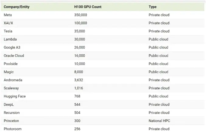
Companies like Meta and Tesla have been purchasing thousands of H100 GPUs to support their ambitious AI initiatives. Although Nvidia has not officially disclosed the pricing for its H100 products, estimates suggest the 80GB version costs between $30,000 and $40,000 each.
Nvidia’s high-performance H100 GPUs have significantly contributed to revenue growth, particularly in the data center sector.
In January 2024, Mark Zuckerberg announced that Meta planned to acquire 350,000 Nvidia H100 GPUs by the end of the year, greatly enhancing the company’s AI computing capabilities.
This massive investment in hardware aims to support Meta in developing advanced AI models, including artificial general intelligence (AGI), a theoretical branch of AI where machines achieve “human-level learning, perception, and cognitive flexibility.”
During Tesla’s Q1 2024 earnings call, CEO Elon Musk revealed that Tesla has 35,000 H100 chips, which will be used for multiple AI projects, including Robotaxi and a supercomputer named Dojo.
While ramping up procurement, most companies in the chart are also advancing their own chip development programs to reduce reliance on Nvidia chips.
For instance, in April of this year, Meta unveiled the latest version of its self-developed chip, MTIA. MTIA is a series of custom chips designed specifically for AI training and inference workloads. Compared to the first-generation AI inference accelerator, MTIA v1, announced last May, the latest version shows significant performance improvements and is tailored for Meta’s social media ranking and recommendation systems. Analysts note that Meta aims to reduce dependence on chip manufacturers like Nvidia.
The name MTIA stands for “Meta Training and Inference Accelerator.” Despite containing “training” in its name, this chip is not optimized for AI training but focuses on inference, which involves running AI models during production.
Meta stated in a blog post that MTIA is a key component of the company’s “long-term plan” to utilize AI for building infrastructure within Meta’s services: “To realize our ambitions for custom chips, we need to invest not only in computing chips but also in memory bandwidth, networking, capacity, and other next-generation hardware systems.”
The new MTIA chip “fundamentally focuses on providing the right balance of computing, memory bandwidth, and memory capacity.” The first-generation MTIA v1 chip uses TSMC’s 7nm process technology, while the new MTIA chip employs TSMC’s 5nm process, featuring more processing cores. The chip will have 256MB of on-chip memory, operating at a frequency of 1.3GHz, compared to MTIA v1’s 128MB and 800MHz. Early test results from Meta indicate that the new chip performs three times better than its predecessor when testing four key models.
In hardware terms, to support the next-generation chips, Meta has developed a large rack system that can accommodate up to 72 accelerators. It consists of three enclosures, each housing 12 boards, with two accelerators per board. This system can boost the chip’s clock frequency from the original 800 MHz to 1.35GHz and operates at 90 watts, compared to the initial design’s 25 watts.
In software terms, Meta emphasizes that the software stack running on the new chip system is very similar to that of MTIA v1, accelerating the deployment speed for teams. Additionally, the new MTIA is compatible with code developed for MTIA v1. Since Meta has integrated the complete software stack into the chip, developers can get up and running with Meta’s traffic in just a few days, enabling Meta to deploy the chip in 16 regions and run production models within nine months.
According to Meta’s summary, the testing results so far indicate that the MTIA chip can handle low complexity (LC) and high complexity (HC) ranking and recommendation models as components of Meta products: “Because we control the entire stack, we can achieve greater efficiency compared to commercial GPUs.”
Currently, the new MTIA chip has been deployed in Meta’s data centers and has shown positive results: “The company is able to invest more computing power for denser AI workloads. The chip has proven to be highly complementary to commercial GPUs in terms of providing the best combination of performance and efficiency for Meta-specific workloads.”
Tesla also relies on Nvidia to power its current Dojo training computer, but it does not want to put all its eggs in one basket—especially given the high prices of Nvidia chips. Tesla aims to produce better products to increase bandwidth and reduce latency. This is why the automotive manufacturer’s AI division has decided to launch its own custom hardware program, aimed at training AI models more efficiently than traditional systems.
At the core of this plan is Tesla’s proprietary D1 chip, which the company claims is optimized for AI workloads.
Tesla introduced the D1 chip at its 2021 AI Day, a palm-sized silicon chip that is now in production. TSMC manufactures the chip using a 7nm process node. Tesla states that the D1 chip contains 50 billion transistors and has a large die size of 645 square millimeters. All of this indicates that the D1 chip is expected to be very powerful and efficient, capable of quickly processing complex tasks.
However, the performance of the D1 chip still falls short compared to Nvidia’s A100 chip, which is also manufactured by TSMC using a 7nm process. The A100 contains 54 billion transistors and has a die size of 826 square millimeters, making it slightly more powerful than Tesla’s D1.
To achieve higher bandwidth and greater computing power, Tesla’s AI team has combined 25 D1 chips into a single block, operating as a unified computing system. Each block has a computing capability of 90 trillion floating-point operations and 36 terabytes per second of bandwidth, containing all the hardware required for power, cooling, and data transfer.
Tesla is also developing the next-generation D2 chip, aimed at addressing information flow bottlenecks. The D2 chip will not connect individual chips together but will integrate the entire Dojo chip onto a single silicon die.

Disclaimer:
- This channel does not make any representations or warranties regarding the availability, accuracy, timeliness, effectiveness, or completeness of any information posted. It hereby disclaims any liability or consequences arising from the use of the information.
- This channel is non-commercial and non-profit. The re-posted content does not signify endorsement of its views or responsibility for its authenticity. It does not intend to constitute any other guidance. This channel is not liable for any inaccuracies or errors in the re-posted or published information, directly or indirectly.
- Some data, materials, text, images, etc., used in this channel are sourced from the internet, and all reposts are duly credited to their sources. If you discover any work that infringes on your intellectual property rights or personal legal interests, please contact us, and we will promptly modify or remove it.