

According to yesterday’s news, as part of the 2024 IEEE VLSI Symposium, Intel recently introduced the technical details of its Intel 3 process node on its official website.
Intel 3 is Intel’s last generation of FinFET transistor technology. Compared to Intel 4, it adds steps using EUV and will be a family of nodes that provide long-term foundry services, including the base Intel 3 and three variant nodes.
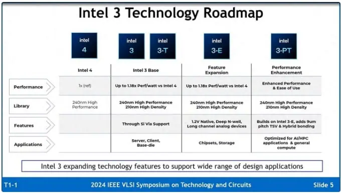
Among them, Intel 3-E natively supports a high voltage of 1.2V, suitable for the manufacture of analog modules. The future Intel 3-PT further enhances overall performance and supports finer 9μm pitch TSV and hybrid bonding.
Intel claims that as its “ultimate FinFET process,” Intel 3-PT will be a mainstream choice for many years, used by internal and external foundry customers alongside angstrom-level process nodes.
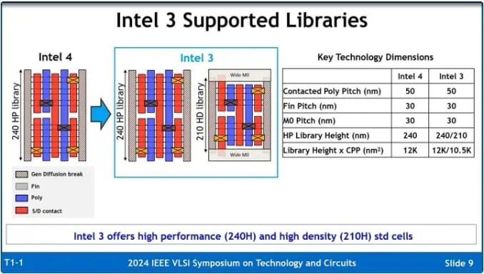
Compared to the Intel 4 process, which only includes a 240nm high-performance library (HP library), Intel 3 introduces a 210nm high-density (HD) library, offering more possibilities in transistor performance orientation.
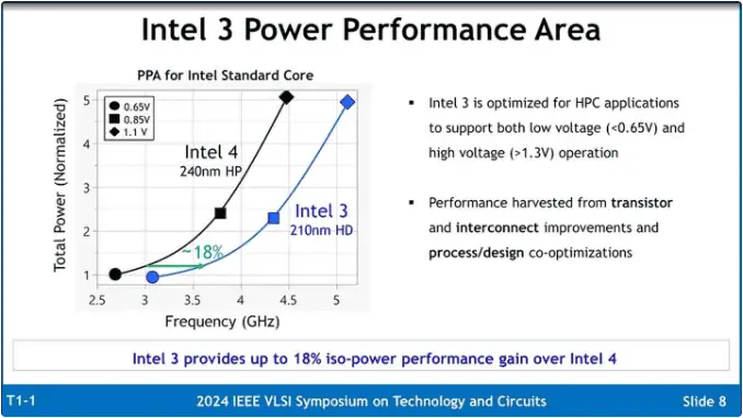
Intel stated that its base Intel 3 process, when using the high-density library, can improve frequency by up to 18% compared to the Intel 4 process.
Additionally, Intel also claims that the density of the base version of the Intel 3 process has increased by 10%, achieving a “full-node” level improvement.
Regarding the metal interconnect layers of the transistors, Intel 3 offers two new options in addition to the 14+2 layers of Intel 4: 12+2 and 19+2, aimed at low-cost and high-performance uses respectively.
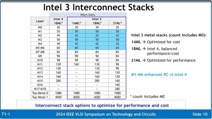
Specifically for each metal layer, Intel has maintained the same pitch as Intel 4 in key layers such as M0 and M1, mainly reducing the pitch of M2 and M4 from 45nm to 42nm.
Related:
- Intel Partners with TSMC for 2nm PC Processor Development
- Hong Kong Customs Seizes 596 High-End CPUs
- Intel Continues Selling Faulty CPUs – No Recall Planned
- Are Supercomputers Only About Maximizing CPU Quantities?
- Intel Explores CEO Options as Leadership Transition Looms

Disclaimer: This article is created by the original author. The content of the article represents their personal opinions. Our reposting is for sharing and discussion purposes only and does not imply our endorsement or agreement. If you have any objections, please get in touch with us through the provided channels.