
In the AI era where technology is prioritized, storage memory will play a more important role.
HBM is High Bandwidth Memory. South Korea’s HBM leader SK Hynix, as a major supplier, has shown remarkable performance. Its market value has soared since 2023, surpassing the $100 billion mark on April 1, 2024. The stock price has also skyrocketed, more than doubling from the beginning of 2023 to April 2024.
In all aspects, HBM has ushered in a new wave of growth momentum for memory manufacturers. American memory giant Micron also stated that HBM capacity was fully booked as soon as it became available. What exactly is HBM, and why has it become a key focus in the AI era?
1. What is HBM? How is it different from traditional DRAM?

Simply put, the stronger the AI processor, the stronger the memory required.
Micron’s Vice President and General Manager of the Compute Products Group in the Compute and Networking Business Unit, Praveen Vaidyanathan, pointed out that chip performance is directly correlated with the bandwidth and capacity of the memory. As the number of parameters in large language models (LLMs) increases, higher bandwidth memory is needed for AI processors to operate smoothly.
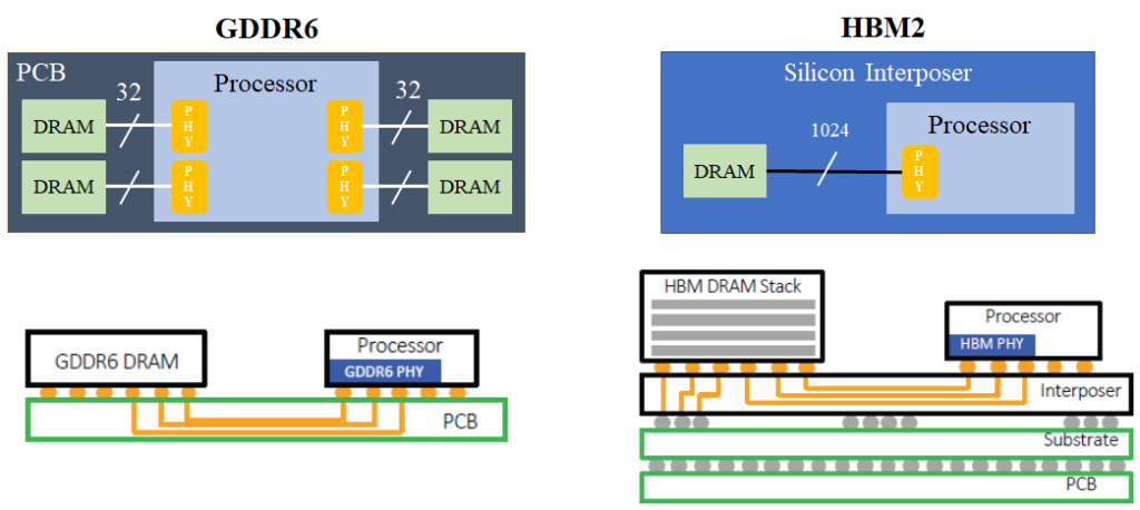
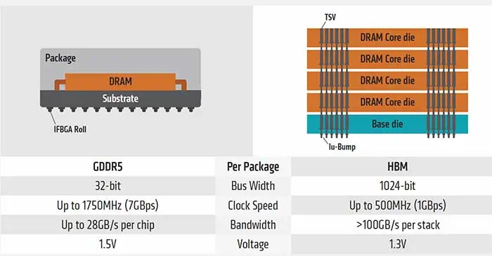
Compared to traditional DRAM, HBM is “high bandwidth” memory. High bandwidth is like a highway: the wider the road, the more traffic it can handle, which means the memory can transfer more data. HBM can be simply understood as multiple DRAMs stacked together through advanced packaging, offering faster transmission speeds and larger storage capacity.
According to SemiAnalysis, GPT-4 alone contains 1.8 trillion parameters. To apply AI, memory like HBM with larger capacity and faster access is necessary to easily transfer and store parameters. However, there is no substitution relationship between HBM and general DRAM; rather, the different application needs have led to the development of this technology.
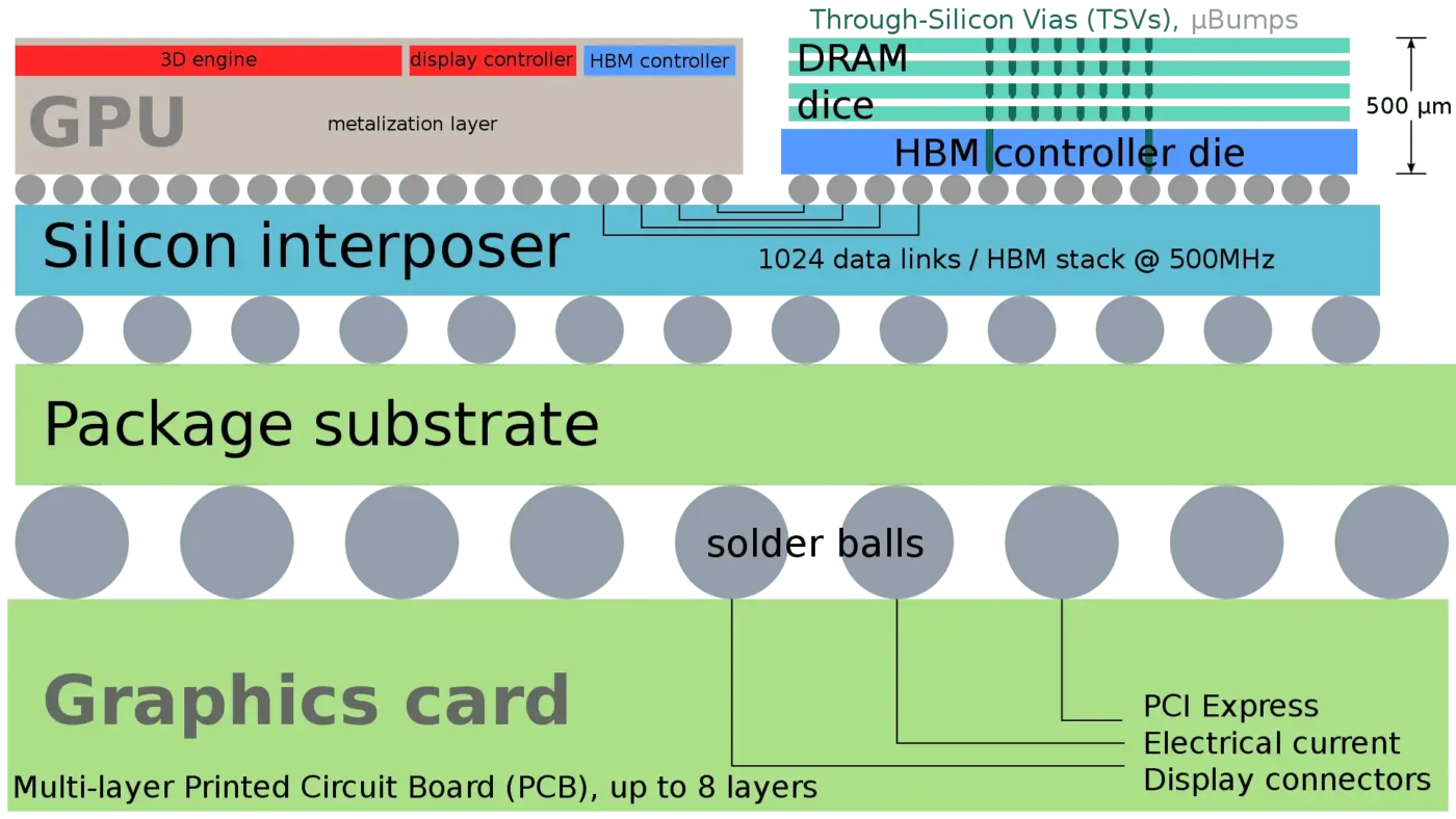
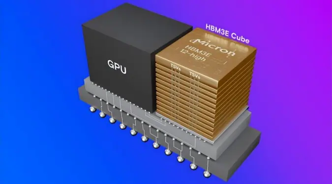
2. HBM 3D Diagram

High Bandwidth Memory (HBM) is created by stacking DRAM using advanced packaging technology and integrating it with the GPU on the same chip, facilitating closer access and data transfer. The primary manufacturing method involves using Through-Silicon Via (TSV) technology, where small holes are drilled into the chip and filled with conductive materials like copper, connecting metal balls to achieve electrical conductivity.
3. What are the technical challenges of HBM?
“Stacking DRAM” sounds simple, but there are several technical difficulties. Vaidyanathan pointed out three key technical challenges affecting yield:
First, thickness.
The thickness of HBM is only half that of a human hair, meaning the thickness of each DRAM layer must be controlled with extremely fine precision. Vaidyanathan noted, “As the number of stacked layers increases, the DRAM must be made thinner.” In this scenario, companies need more advanced DRAM processes to achieve this.
Second, the precision of wafer stacking.
HBM packaging involves aligning each DRAM wafer before cutting, with the resulting dies being HBM. To make the stack thinner, manufacturers drill through the silicon wafer and fill it with conductive materials to achieve electrical connectivity, replacing the traditional wire bonding. This drilling technique is called “Through-Silicon Via (TSV).”
For a four-layer HBM stack, the silicon vias (TSV) must be precisely aligned from the start of wafer stacking and cutting. “If there is any misalignment during cutting, it won’t conduct electricity,” Vaidyanathan said. Achieving this requires highly precise silicon via technology.
Third, the heat dissipation problem after stacking.
HBM was invented to integrate memory and processors, including CPUs and GPUs, into a single IC. This reduces the distance between memory and processor significantly, making heat dissipation a critical issue. Given these three points, the importance of packaging technology is more crucial than ever.
What are the applications of HBM? Besides AI servers, where else is HBM used?
Due to the high technical difficulty, HBM also has a relatively high cost. HBM was first developed in 2013 by AMD and SK Hynix, but it was rarely adopted by chipmakers due to its high price. It has only recently gained significant attention due to AI applications.
Industry experts analyze that although the price of more advanced HBM is higher, manufacturers are willing to invest in it as long as it is efficient and energy-saving.
Currently, AI servers are the most important market for HBM. Micron and SK Hynix’s HBM3e has been validated by Nvidia, and there are reports that Nvidia has paid hundreds of millions of dollars in advance to secure supply. Vaidyanathan noted, “The memory required for AI servers is 5 to 6 times that of traditional servers.”
Additionally, the smart driving car market is another important application scenario for HBM. A report published by Mordor Intelligence indicated that ADAS (Advanced Driver Assistance Systems) is driving the demand for HBM. Considering this, the demand for HBM in AI servers and automotive applications may last for up to 10 years.
4. The Battle Behind HBM Memory
The war among memory giants over HBM has already begun. TrendForce noted that in 2022, SK Hynix took the lead with nearly 50% of the global HBM market share, followed by Samsung with 40%, and Micron with 10%. According to BusinessKorea, Samsung plans to aggressively expand HBM production in 2024 to catch up with SK Hynix. Although Micron appears to be trailing, it aims to make a comeback in the HBM arena through technological advancements.
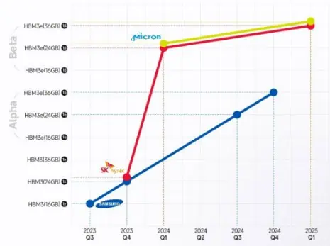
Similar to TSMC’s 3nm and 5nm processes, DRAM also has process iterations, listed as 1y, 1z, 1α (1-alpha), 1β (1-beta), and 1γ (1-gamma). Among these, 1β is the most advanced memory currently in mass production, while 1γ is yet to be produced. In comparison, the latest generation HBM3e uses the 1α process by Samsung, while SK Hynix and Micron use 1β, giving them a technological edge over Samsung. Investment bank analysts point out that Micron hopes to leverage its technical superiority in HBM to seize market leadership.
The global memory market has long been dominated by three major players, but the growing importance of HBM could usher in a new phase, potentially reshaping the competitive landscape. In the AI era, where advanced technology is prioritized and cost is secondary, memory will play a more critical role than ever before.

Disclaimer: This article is created by the original author. The content of the article represents their personal opinions. Our reposting is for sharing and discussion purposes only and does not imply our endorsement or agreement. If you have any objections, please contact us through the provided channels.