

The AI wave has placed higher demands on memory, highlighting the importance of high-capacity, high-performance storage products, and intensifying the competition in storage industry technology and production capacity. In the NAND Flash sector, the number of flash memory stack layers continues to increase; in the DRAM sector, HBM production is expanding continuously with ongoing technological iterations, and the potential of 3D DRAM is attracting significant attention; a new type of storage technology that combines the advantages of DRAM and NAND Flash is being mentioned again by the original manufacturers; while PCIe 5.0 has not yet become widespread, PCIe 7.0 is already gearing up…

01
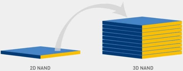
Samsung begins mass production of its ninth-generation V-NAND flash memory

Samsung has recently announced the mass production of its ninth-generation V-NAND 1Tb TLC products. Later this year, Samsung will begin mass production of the ninth-generation V-NAND with four-level cell (QLC) technology.
Compared to the previous eighth-generation V-NAND, the ninth-generation V-NAND 1Tb TLC products have approximately 50% higher bit density and a 10% reduction in power consumption. Additionally, Samsung has improved production efficiency through channel hole etching technology, which creates electronic pathways by stacking die layers and allows drilling in a dual-layer structure, achieving Samsung’s highest number of cell layers and maximizing manufacturing productivity.
The ninth-generation V-NAND is equipped with the next-generation NAND flash interface, “Toggle 5.1,” which increases data input/output speed by 33%, reaching up to 3.2 gigabits per second (Gbps). Samsung states that with the latest V-NAND, it will continue to innovate in the high-performance, high-density SSD market to meet the demands of the upcoming AI era.
Samsung’s press release did not specify the number of layers for the ninth-generation V-NAND. Industry sources had previously stated that Samsung’s eighth-generation V-NAND had 236 layers, and the ninth-generation V-NAND is expected to have 290 layers.
Besides Samsung, other manufacturers like Micron, SK Hynix, and Kioxia/Western Digital are also continuously increasing the number of NAND stack layers. From the actions of these manufacturers, it is clear that 200 layers are not the limit; Samsung plans to achieve 1000 layers of NAND Flash by 2030, while Kioxia aims to mass-produce more than 1000 layers of 3D NAND Flash chips by 2031.
02
HBM4 is expected to be in production by 2026.

Currently, the HBM market is dominated by HBM3, with HBM3e expected to increase in volume quarter by quarter in the second half of the year, gradually becoming mainstream. Major manufacturers are mainly focusing on expanding production of HBM3 and HBM3e products.
At the same time, to continuously improve performance and meet the needs of future applications such as AI, manufacturers have already begun developing the next generation of HBM.
In April, SK Hynix announced a partnership with TSMC to develop HBM4, which is expected to enter production in 2026.
It is reported that the two companies will first focus on performance improvements for the base die, which is located at the lowest layer within the HBM package. Previous HBM products from SK Hynix, including HBM3E (the fifth-generation HBM product), were based on the company’s manufacturing processes. However, starting with the HBM4 product, they plan to adopt TSMC’s advanced logic processes. Using ultra-fine processes on the base die can add more functionality. As a result, the company plans to produce customized HBM products that more broadly meet customer needs in terms of performance and efficiency.
Meanwhile, the two companies will collaborate to optimize the integration of SK Hynix’s HBM products and TSMC’s CoWoS technology to meet the requirements of HBM-related customers.
03
Will the era of 3D DRAM begin in 2025?
Compared to traditional DRAM, 3D DRAM allows direct data access and writing through vertically stacked storage cells, improving access speed, while also offering advantages in high capacity, high speed, low power consumption, and high reliability.
Currently, the competition in DRAM technology focuses on advanced processing technologies. As technology nodes progress towards 10nm, existing design solutions are reaching their limits, prompting manufacturers to actively explore 3D DRAM.
At the Memcon 2024 conference, Samsung showcased two new 3D DRAM technologies, including Vertical Channel Transistor (VCT) and Stacked DRAM.
Samsung stated at the conference that it expects to lead the industry into the era of 3D DRAM after 2025. It is reported that Samsung will first introduce VCT technology, and later, between 2030-2031, upgrade to Stacked DRAM, stacking multiple groups of VCTs together to continuously enhance DRAM capacity and performance.
04
Kioxia Targets SCM
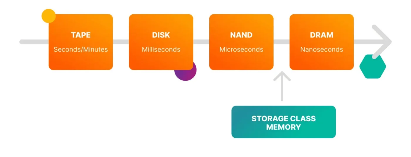
In April, Kioxia’s CTO, Hidefumi Miyajima, stated that compared to competitors who operate both NAND and DRAM, Kioxia is at a competitive disadvantage in terms of business diversity. There is a need to develop new storage product businesses like Storage Class Memory (SCM), especially as the gap between memory and flash storage performance widens under the AI boom, and SCM is expected to bridge this gap.
To strengthen advanced storage technology, Kioxia also recently reorganized its “Memory Technology Research Laboratory” into the “Advanced Technology Research Laboratory.”
Data shows that SCM combines the characteristics of DRAM and flash memory, possessing the high-speed read/write performance of DRAM and the persistent storage capabilities of NAND flash. It aims to address the issues of small capacity, volatility, and high cost associated with DRAM while meeting the needs for high-speed read/write and persistent storage. SCM products mainly include PCM, ReRAM, MRAM, and NRAM.
In the field of SCM, Kioxia is primarily focusing on the XL-FLASH storage solution. Like all flash storage, XL-FLASH retains data when power is cut off. Additionally, it features extremely low latency and high performance, bridging the performance gap between volatile memory (such as DRAM) and current flash memory. In 2022, Kioxia launched the second generation of XL-FLASH, which supports MLC mode.
With Kioxia’s renewed focus on SCM, the industry believes that Kioxia’s SCM research will concentrate on new storage types such as MRAM and ReRAM, with related products expected to be launched within the next 2 to 3 years.
05
The PCIe 7.0 specification is expected to be released next year.

PCIe is a high-speed serial computer expansion bus standard used for data transfer between expansion cards and computer motherboards. Due to its high speed, high bandwidth, and low latency characteristics, this technology is widely used in various hardware devices, including storage.
As PCIe technology continues to evolve, its performance also improves. In the storage sector, consumer and enterprise markets have widely adopted PCIe standard SSD products. The highest commercially available specification currently is PCIe 5.0 SSD. As the fifth generation of PCIe technology, its speed is twice that of PCIe 4.0, and its power consumption has been reduced by about 30%. Additionally, PCIe 5.0 supports up to 16 lanes of connection. In an x16 lane configuration, the maximum theoretical bandwidth of PCIe 4.0 is 64GB/s, while PCIe 5.0 can reach 128 GB/s.
| Revision | Max Data Rate | Encoding | Signaling |
|---|---|---|---|
| PCIe 7.0 (2025) | 128.0 GT/s | 1b/1b (Flit Mode*) | PAM4 |
| PCIe 6.0 (2022) | 64.0 GT/s | 1b/1b (Flit Mode*) | PAM4 |
| PCIe 5.0 (2019) | 32.0 GT/s | 128b/130b | NRZ |
| PCIe 4.0 (2017) | 16.0 GT/s | 128b/130b | NRZ |
| PCIe 3.0 (2010) | 8.0 GT/s | 128b/130b | NRZ |
| PCIe 2.0 (2007) | 5.0 GT/s | 8b/10b | NRZ |
| PCIe 1.0 (2003) | 2.5 GT/s | 8b/10b | NRZ |
Following PCIe 5.0, the PCIe 6.0 standard has also been announced, which doubles the bandwidth compared to PCIe 5.0. Recently, the PCIe standards organization, PCI-SIG, announced the PCIe 7.0 specification version 0.5. Compared to the PCIe 6.0 standard, PCIe 7.0 doubles the rate again while continuing to use PAM4 signal modulation, achieving a raw data rate of 128GT/s and a bidirectional bit rate of 512GB/s in an x16 configuration.
Additionally, PCIe 7.0 supports 800 Gigabit Ethernet, meeting the needs of high-end applications such as artificial intelligence and machine learning, high-performance computing, quantum computing, hyperscale data centers, and cloud platforms.
PCI-SIG indicates that, given the current progress of development, the formal version 1.0 of the PCIe 7.0 specification is expected to be released within 2025.
06
Words in the End
Under the strong drive of AI, the memory market continues to benefit. Currently, HBM is undoubtedly the most focused product, with a market situation where supply cannot meet demand, and its output value continues to rise. The global market research institute TrendForce previously projected that in 2023, HBM’s share of the total DRAM industry’s output value would be about 8.4%, and by the end of 2024, it would expand to 20.1%.
In the future, as storage technology continues to break through and new applications emerge, who will become the next “darling” of the memory market? We can wait and see.

Disclaimer: This article is created by the original author. The content of the article represents their personal opinions. Our reposting is for sharing and discussion purposes only and does not imply our endorsement or agreement. If you have any objections, please contact us through the provided channels.