
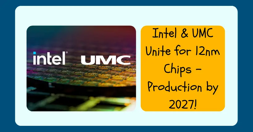
On January 25th, Intel and United Microelectronics Corporation (UMC) jointly announced the establishment of a partnership. The collaboration will focus on the manufacturing of chips based on a 12-nanometer process.
This agreement allows for a combination of Intel’s chip manufacturing facilities and capacity in the United States with UMC’s rich experience in mature process chip manufacturing. This aims to achieve the optimal combination of process and capacity, leading to a mutually beneficial and complementary partnership.
Currently, Intel’s chip foundry division has three factories at the Ocotillo Technology manufacturing base in Arizona, working with 12, 22, and 32-nanometer wafers.
These factories have been in operation for many years, primarily manufacturing 14-nanometer process chips. However, the processes have gradually become outdated. Nevertheless, it’s possible to upgrade and transform these existing manufacturing equipment and processes to produce 12-nanometer chips.
The collaboration between Intel and TSMC primarily revolves around this aspect. Both parties will jointly upgrade the existing production lines, and then use these factories to manufacture 12-nanometer chips. For Intel, most of the existing equipment can continue to be used, potentially reducing costs by at least 90%.
UMC holds many advantages in this area. It can assist Intel with the upgrades and modifications of the existing equipment. Additionally, it can bring new business to Intel’s chip foundry division. For example, in the future, both parties could jointly manufacture RF and WiFi chips, expanding the manufacturing scope of chip foundry services and increasing profits.
UMC also benefits from this partnership. The primary production equipment is provided by Intel and is already in place, which greatly helps UMC to expand its chip business in the United States at a low cost and with ease.
It is reported that once the upgrades and transformations of these three factories are completed, the future 12-nanometer chips produced will not be for Intel’s use. Instead, like competitors TSMC and Samsung, they will undertake contracts for third-party companies to manufacture chips.
Although the most advanced mainstream chip processes have reached 3 nanometers, making 12-nanometer processes seem outdated, this is not necessarily the case.
As the saying goes, “More pixels don’t always mean better, and more cameras don’t always mean better.” Similarly, more advanced chip processes are not always better. Apart from smartphone processors and a few other applications, most applications do not require very advanced, high-performance chips; adequacy is sufficient. For these applications, the cost of chip manufacturing is more important than performance.
Therefore, there is still a significant demand in the market for 12-nanometer and even 28-nanometer chips, such as those used in various mobile communication infrastructures and network devices.
Moreover, the overall process for 12-nanometer chip foundry services is now very mature and standardized, using industry-standard design tools (EDA) and process design kits (PDK). This is very user-friendly for third-party companies with chip foundry needs.
In summary, Intel has ready-to-use chip manufacturing factories and equipment, while UMC has years of in-depth experience in the chip foundry service field, particularly in mature chip manufacturing processes (including 12 nanometers), along with numerous channels and customers.
Thus, this collaboration has strong complementarity. With upgrades and transformations to Intel’s existing production facilities, they can be put into commercial use for benefits.
Nevertheless, upgrading existing equipment is not an easy task and may take two to three years to complete. It’s expected that production will officially start in 2027, focusing on manufacturing 12-nanometer chips.
Related:
- HKMG Technology: Key to Sub-28nm Advanced Node Success
- Intel Big Move: Foundry Business Spin-Off and Layoffs!
- Intel NM Launch: Pioneering 3D Foveros Chip Production
- Samsung 1b DRAM Yield Below Target, New Task Force
- Talent Exodus from South Korea Semiconductor Industry
- Is the Move to 5nm Chip Technology Part of a Conspiracy?
- Infineon Launches Construction of Thai Power Module Plant

Disclaimer: This article is created by the original author. The content of the article represents their personal opinions. Our reposting is for sharing and discussion purposes only and does not imply our endorsement or agreement. If you have any objections, please get in touch with us through the provided channels.