
In recent months, Intel has made a lot of progress in improving chip manufacturing processes and expanding chip factories. The overall development speed is very fast and impressive.
The progress that still only exists in Intel’s PPT promotional materials and lacks solid evidence will not be mentioned by the editor now. Below, only two recent developments that everyone can see and touch are mentioned.
On December 21, 2023, Intel received the first 2nm lithography machine delivered by the Dutch lithography giant ASML. Please refer to Figure 1. A while ago, Intel’s CEO Pat Gelsinger (Figure 2) revealed that the company’s wafer fab near Magdeburg, Germany, is about to start production and will produce the Intel 18A process, which is the 2nm (including below 2nm) process chips.
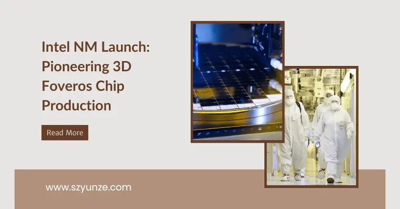
On January 24, Intel announced another significant recent development in this field. Its Rio Rancho chip factory in New Mexico, USA (see the picture below) has recently been officially put into operation, with a total investment of about 3.5 billion US dollars.
Keyvan Esfarjani, Intel’s Executive Vice President and Chief Global Operations Officer, stated:
“Today, we warmly celebrate the official commissioning of Intel’s Rio Rancho chip factory in New Mexico. It is currently the only factory in the United States that uses the world’s most advanced packaging solutions to manufacture chips.
This cutting-edge technology (Foveros 3D) sets Intel apart, enabling us to bring great advantages to our customers in terms of chip performance, size, and flexibility.”
Intel revealed that its Fab 9 and Fab 11x in Rio Rancho will be the first to mass-produce chips using its Foveros 3D packaging technology.
Foveros 3D (see the picture above) is Intel’s next-generation advanced 3D chip packaging solution, supporting the use of vertically stacked, rather than side-by-side, small chips to make chips. In addition, this technology can also reduce coupling, supporting Intel and other chip foundries (such as TSMC and GlobalFoundries) to manufacture parts of small chips separately, and then package them together to improve chip manufacturing efficiency and reduce costs.
Intel stated that by comprehensively using advanced packaging technologies such as Foveros 3D and EMIB (Embedded Multi-die Interconnect Bridge), it will be possible to manufacture chips containing 1 trillion transistors in the future, and even after 2030, the semiconductor industry can continue to roughly follow Moore’s Law for rapid development.
In addition, with the official commissioning of this chip factory, it is expected to create hundreds of jobs in New Mexico, more than 3,000 construction jobs, and another 3,500 jobs.
It is reported that this chip factory in New Mexico is just a small part of Intel’s grand strategic layout to improve chip processes and output in the United States, just an appetizer. In addition to this, Intel is also building multiple wafer fabs in Arizona, Ohio, and other places, demonstrating great ambition.
From the various known signs, Intel’s investment in improving chip processes and output is very large, the development speed is fast, and it is very steady. In the next two to three years, it is very likely to catch up with TSMC and Samsung.

Related:
- Intel Big Move: Foundry Business Spin-Off and Layoffs!
- Intel & UMC Unite for 12nm Chips – Production by 2027!
