

01
What is ASIC (Application Specific Integrated Circuit)?
The parallel computing power of GPUs is strong, but it also has drawbacks, such as high power consumption, large size, and expensive prices.
After entering the 21st century, there have been two significant trends in computing power demand: first, the segmentation of computing power usage scenarios; second, increasing user demands for computing power performance. General-purpose computing chips are no longer able to meet user needs.
As a result, more and more companies are intensifying their research and investment efforts in specialized computing chips. ASIC (Application Specific Integrated Circuit) is a type of chip designed specifically for particular tasks.
The official definition of ASIC refers to a circuit specially designed and manufactured for specific user requirements or the needs of specific electronic systems.
ASIC emerged in the 1970s and 1980s. In its early days, it was used in computers. Later, it was mainly used in embedded control. In recent years, as mentioned earlier, it has begun to rise in use for AI inference, high-speed searches, as well as vision and image processing.
When discussing ASIC, it’s inevitable to mention Google’s well-known TPU.
TPU, short for Tensor Processing Unit, is a tensor processing unit. The term ‘tensor’ refers to a mathematical entity that contains multiple numbers (multi-dimensional arrays).
Currently, almost all machine learning systems use tensors as their basic data structure. Therefore, we can simply understand the tensor processing unit as an ‘AI processing unit.’
In 2015, to better fulfill its deep learning tasks and enhance AI computing power, Google introduced a chip specifically designed for neural network training, namely TPU v1.
As compared to traditional CPUs and GPUs, TPU v1 brings a substantial impact to the industry in neural network computations, offering a performance boost of 15 to 30 times and an efficiency increase of 30 to 80 times.
In 2017 and 2018, Google continued its momentum by releasing more powerful versions, TPU v2 and TPU v3, dedicated to AI training and inference. In 2021, they launched TPU v4, employing a 7nm process with 22 billion transistors, providing a tenfold performance increase compared to its predecessor and surpassing Nvidia’s A100 by 1.7 times.
Apart from Google, several major companies have been delving into ASIC technology in recent years.
In late 2019, Intel acquired the Israeli AI chip company, Habana Labs, and in 2022, they unveiled the Gaudi 2 ASIC chip. IBM Research also introduced an AI ASIC chip named AIU by the end of 2022.
Samsung previously ventured into ASICs a few years back, specifically developing chips for mining machines. Indeed, many recognize ASICs from their inception in Bitcoin mining. Compared to GPU and CPU mining, ASIC miners are more efficient and consume less power.
Apart from TPUs and mining machines, there are two other well-known types of ASIC chips: DPUs and NPUs.
DPU stands for Data Processing Unit, primarily used in data centers. It was previously elaborated upon by Xiao Zao, and more information can be found here: What Exactly is the DPU That’s All Over the Internet?
As for NPUs, they are Neural Processing Units, that simulate human neurons and synapses at the circuit level and process data using deep learning instructions. NPUs are specifically designed for neural network inference and efficiently perform operations like convolution and pooling. Many smartphone chips often integrate NPUs.
Speaking of smartphone chips, it’s worth noting that our current mobile device’s main chip, often referred to as the SoC chip, is, in fact, a type of ASIC chip.
Where do ASIC‘s advantages as custom chips lie? Are they limited to exclusive use by enterprises, specific logos, and naming?
Not quite.
Customization is akin to tailoring a suit. Based on the specialized tasks targeted by the chip, its computing power and efficiency are precisely aligned with the task’s algorithms. The core count, the ratio of logic computation units to control units, the inclusion of caches, and the entire chip architecture are all meticulously tailored.
As a result, specialized custom chips can achieve the utmost in size and power efficiency. The reliability, confidentiality, computing power, and efficiency of such chips will surpass those of general-purpose chips (CPU, GPU).
One might notice that the ASIC companies mentioned earlier are major players like Google, Intel, IBM, and Samsung. This is because custom chip design demands exceptionally high levels of R&D expertise and entails enormous capital investment.
Developing an ASIC chip involves complex design processes such as code design, synthesis, and backend, followed by several months of production, assembly, and testing before obtaining the chip for system integration.
Many are familiar with “tape-out.” Similar to a production line, manufacturing a chip through a series of technological steps is tape-out, essentially a trial production.
The development of ASICs necessitates tape-out. For instance, a single tape-out at 14nm technology requires around $3 million. At 5nm technology, this cost escalates dramatically to as high as $47.25 million.
A failed tape-out results in a complete waste of money and considerable time and effort. Smaller companies simply cannot afford such risks.
However, does this mean smaller companies cannot engage in chip customization?
Certainly not. Next up is another game-changer – the FPGA
02
What is FPGA (Field Programmable Gate Array)?
FPGAs, with the full English name Field Programmable Gate Array, have been trending in industries in recent years, exhibiting a momentum even stronger than ASICs, often dubbed as the “universal chip.”
In essence, an FPGA is a reconfigurable chip. It allows for unlimited reprogramming post-manufacture based on user requirements to achieve desired digital logic functions.
The reason behind FPGA‘s DIY capabilities lies in its unique architecture.
An FPGA comprises three types of programmable circuits: Configurable Logic Blocks (CLBs), Input/Output Blocks (IOBs), and Programmable Interconnect Resources (PIRs), along with static memory SRAM.
- CLBs, the most crucial component in FPGAs, form the fundamental unit for implementing logic functions and support the primary circuit functions. These CLBs are typically organized in a grid known as the Logic Cell Array (LCA) spread across the chip.
- IOBs serve to interface the logic on the chip with external pins and are generally situated around the chip’s perimeter.
- PIRs offer abundant interconnection resources, including vertical and horizontal grid-like connections, programmable switch matrices, and programmable connection points. They establish connections that form specific functional circuits.
The static memory SRAM stores programming data for internal IOBs, CLBs, and PIRs, controlling them to accomplish system logic functions.
CLBs themselves consist mainly of Look-Up Tables (LUTs), Multiplexers, and Flip-Flops. They carry individual logic “gates” within circuits, enabling the implementation of complex logic functions.
In essence, LUTs can be seen as RAM storing computed results. When a user describes a logic circuit, the software calculates all possible outcomes and writes them into this RAM. Every signal undergoing logical operations is akin to inputting an address to perform a table lookup. The LUT fetches the content corresponding to the address and returns the result.
This hardware-based computational method offers faster processing speeds.
When users utilize FPGAs, they complete circuit designs using Hardware Description Languages (such as Verilog or VHDL). Subsequently, they “program” (burn) the FPGA, loading the design onto it to achieve the corresponding functionality.
Upon powering up, the FPGA reads data from Electrically Programmable Read-Only Memory (EPROM) into SRAM. Once configured, the FPGA enters its operational state. Upon power loss, the FPGA reverts to a blank slate, losing its internal logic relationships. This cyclical process enables “on-site” customization.
The potential of FPGAs is robust. In theory, given a large enough gate circuit scale provided by the FPGA, programming could realize the logic functions of any ASIC.
Let’s take a closer look at the developmental journey of FPGAs.
FPGA, an offspring of programmable devices like PAL (Programmable Array Logic) and GAL (Generic Array Logic), falls into the category of semi-custom circuits.
It emerged in 1985 with Xilinx being its inventor. Later, companies such as Altera, Lattice, and Microsemi also ventured into the FPGA domain, eventually shaping the industry with four major players.
In May 2015, Intel made a significant move by acquiring Altera for a staggering $16.7 billion, subsequently integrating it into the Programmable Solutions Group (PSG) division.
In 2020, Intel‘s competitor, AMD, not to be outdone, acquired Xilinx for $35 billion.
Consequently, the landscape evolved to feature four dominant players: Xilinx (under AMD), Intel, Lattice, and Microsemi, maintaining a similar market structure.
By 2021, these four companies held market shares of 51%, 29%, 7%, and 6%, collectively capturing 93% of the global market.
Recently, in October 2023, Intel announced plans to separate the PSG division, intending to operate it as an independent entity.
Regarding domestic FPGA manufacturers in China, there are several, including Fudan Microelectronics, SMIC (Semiconductor Manufacturing International Corporation), Anlogic, Dongtu Technology, Gowin Semiconductor, JingMicro, JingMicro YaGe, ZhiDuojing, and AogeXin. Although the quantity appears substantial, there’s a considerable gap in their technological capabilities.
03
ASIC and FPGA Differences
Let’s focus on distinguishing ASIC from FPGA and also their distinctions from CPUs and GPUs.
ASIC and FPGA are fundamentally both chips. ASICs are fully customized chips with fixed functionality, impossible to alter once designed. In contrast, FPGAs are semi-custom chips with flexible functionality, offering greater versatility.
An illustrative analogy to comprehend the difference between the two:
ASICs are akin to using a mold to create a toy. Preparing the mold is labor-intensive, and once it’s established, modifications become impossible. If a new toy design is desired, a new mold is necessary.
On the other hand, FPGAs are like constructing toys using Lego bricks. They are easy to start with, and quick to assemble. If unsatisfied with the result or seeking a new design, one can disassemble and create anew.
Many design tools used for ASIC and FPGA are similar. However, in the design process, FPGA is less intricate than ASIC, excluding certain manufacturing processes and additional design verification steps, encompassing about 50-70% of the ASIC process. The complex tape-out process required for ASICs is unnecessary for FPGAs.
This implies that developing an ASIC might require several months to over a year, while FPGA development typically demands only a few weeks to a few months.
Earlier, it was mentioned that FPGAs do not require tape-out. Does this mean that FPGA costs are always lower than ASICs?
Not necessarily.
FPGAs can be programmed and prototyped in labs or on-site without incurring Non-Recurring Engineering (NRE) costs. However, as a “general-purpose toy,” its cost is about 10 times that of an ASIC (the “molded toy”).
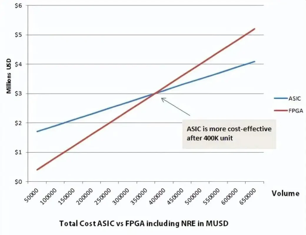
For lower production volumes, FPGAs might be more cost-effective. Conversely, for higher volumes where the one-time engineering costs of ASICs can be amortized, ASICs might be more economical.
It’s similar to mold costs—expensive to create initially, but cost-effective for large-scale production.
As depicted in the figure below, 400,000 units are a tipping point for the cost comparison between ASICs and FPGAs. For volumes below 400,000 units, FPGAs are cheaper; for volumes exceeding this threshold, ASICs become more economical.
From the perspective of performance and power consumption, as a specialized custom chip, ASIC is indeed stronger than FPGA.
FPGAs are universal and editable chips, often containing redundant functionalities. Regardless of the design, there will typically be some surplus components.
As mentioned earlier, ASICs are tailored specifically without waste, employing hard-wired connections. Hence, they offer higher performance and lower power consumption.
FPGA and ASIC do not simply compete or substitute each other; they serve different purposes.
FPGAs are commonly used for product prototyping, design iterations, and specific low-volume applications. They are suitable for products requiring short development cycles. Additionally, FPGAs are often employed for ASIC validation.
ASICs, on the other hand, are used for designing large-scale, high-complexity chips or products with high maturity and larger production volumes.
FPGAs are particularly suitable for beginners’ learning, and competitions, and are widely used in electronic courses across many universities.
Looking at it from a commercial perspective, the primary application areas for FPGAs include communications, defense, aerospace, data centers, healthcare, automotive, and consumer electronics.
FPGAs have long been utilized in the communication sector. Many base station processing chips (baseband processing, beamforming, transceiver units, etc.) leverage FPGAs. They’re also utilized for encoding and protocol acceleration in the core network. Previously, data centers used FPGAs in components like DPUs.
However, as many technologies matured and standardized, telecommunication equipment manufacturers started substituting FPGAs with ASICs to reduce costs.
It’s noteworthy that in recent years, the Open RAN concept has gained popularity, employing general-purpose processors (such as Intel CPUs) for computing. However, this approach’s energy consumption is significantly higher compared to FPGAs and ASICs. This is a primary reason why equipment manufacturers like Huawei are reluctant to embrace Open RAN.
In the automotive and industrial sectors, FPGAs are valued for their latency advantages, often used in Advanced Driver-Assistance Systems (ADAS) and servo motor drives.
FPGAs are used in consumer electronics due to the rapid iteration of products. The lengthy development cycle of ASICs often results in delayed product releases, prompting the preference for FPGAs where faster iterations are possible.
04
FPGA, ASIC, GPU – Which is the most suitable AI chip?
Lastly, let’s circle back to the topic of AI chips.
Firstly, it’s crucial to remember that purely from a theoretical and architectural perspective, the performance and cost-effectiveness of ASICs and FPGAs are undoubtedly superior to CPUs and GPUs.

CPU and GPU follow the Von Neumann architecture, where instructions pass through steps like storage, decoding, execution, and shared memory usage involving arbitration and caching.
However, FPGA and ASIC do not adhere to the Von Neumann architecture (they follow the Harvard architecture). Taking FPGA as an example, its architecture is fundamentally devoid of instructions and shared memory requirements.
The functionality of FPGA‘s logic units is predetermined during programming, representing hardware implementation of software algorithms. For maintaining states, the registers and on-chip memory (BRAM) in FPGA operate under their respective control logic, without the need for arbitration and caching.
Considering the proportion of ALU (Arithmetic Logic Unit) units, GPUs exhibit a higher ratio compared to CPUs. Due to the absence of control modules in FPGAs, all modules are essentially ALU units, resulting in a higher ALU ratio compared to GPUs.
Hence, from various aspects, FPGA‘s computational speed tends to be faster than GPUs.
Now, let’s examine power consumption.
GPUs are notorious for their high power consumption, with a single chip reaching up to 250W or even 450W (like the RTX 4090). In contrast, FPGAs typically consume only around 30 to 50W.
This substantial power difference is primarily due to memory access. GPUs boast extremely high memory interface bandwidth (GDDR5, HBM, HBM2), approximately 4-5 times that of a traditional DDR interface on an FPGA. However, in terms of the chip itself, accessing DRAM consumes over 100 times more energy than SRAM. Frequent DRAM access by GPUs leads to significantly higher power consumption.
Additionally, FPGA‘s operating frequency (below 500MHz) is lower than that of CPUs and GPUs (1-3GHz), contributing to its lower power consumption. The lower working frequency of FPGAs is mainly limited by routing resources. Some lines need longer routes, and a higher clock frequency results in insufficient time for signal propagation.
Lastly, let’s consider latency.
The latency of GPUs is higher than FPGAs.
GPUs typically require dividing different training samples into fixed-sized “batches.” To maximize parallelism, several batches need to be accumulated before simultaneous processing.
FPGA architecture operates in a “Batch-less” manner. It can output immediately upon processing each data packet, thereby having an advantage in terms of latency.
Now, the question arises: If GPUs are inferior to FPGAs and ASICs in various aspects, why have they become the current hot trend in AI computing?
The answer is straightforward. In the relentless pursuit of computational performance and scale, the industry currently pays little attention to costs and power consumption.
Thanks to NVIDIA‘s persistent efforts, GPU core counts and operating frequencies have consistently increased, and chip sizes have grown larger, geared towards sheer computational power. Power consumption is managed through fabrication processes and passive cooling like water cooling, as long as they don’t catch fire.
In addition to hardware advancements, as mentioned earlier, NVIDIA has strategically invested in software and ecosystem development.
Their development of CUDA has been a core competitive advantage for GPUs. With CUDA, even beginners can quickly start GPU development. Over years of dedicated efforts, NVIDIA has built a strong community base.
In comparison, the development process for FPGAs and ASICs remains too complex, making them less suitable for widespread adoption.
In terms of interfaces, while GPUs have relatively uniform interfaces (mainly PCIe), lacking the flexibility of FPGAs (which can easily adapt to standard and non-standard interfaces due to their programmability), it suffices for servers—they can be plugged in and used.
Apart from FPGAs, the reason ASICs lag behind GPUs in AI applications is closely tied to their high costs, excessively long development cycles, and significant development risks. In the rapidly evolving landscape of AI algorithms, ASICs‘ development cycles are a significant challenge.
Considering the above reasons collectively, GPUs have achieved their current prominent position.
In AI training, GPUs exhibit robust computational power, significantly boosting efficiency.
For AI inference, where inputs are typically single objects (such as images), the requirements are lower, and parallelism isn’t as crucial. Thus, the computational advantage of GPUs isn’t as prominent. Many enterprises might opt for cheaper and more power-efficient options like FPGAs or ASICs for computation.
Similar considerations apply to other computational scenarios. GPU is the first choice for those emphasizing absolute computational performance. For scenarios where computational performance demands are lower, FPGAs or ASICs, which offer potential cost savings, might be considered.
05
Words in the end
This concludes the overview of CPU, GPU, FPGA, and ASIC—representatives of computational chips. Presently, these chips are responsible for nearly all computational scenarios in the human domain.
With the evolution of technology, new trends are emerging in computational chips. For instance, there’s a trend toward heterogeneous computing, where different types of computational chips are combined to leverage their respective strengths. Another significant development is the advent of neuromorphic chips led by IBM, which emulate synaptic connections in the brain, simulating human brain processes—a breakthrough that’s gaining traction. I’ll delve deeper into these topics in the future.
I hope SZYUNZE’s series of articles on chips has been helpful to everyone. If you’ve found them interesting, I’d appreciate your following, sharing, and liking.
Thank you!
Related:

Disclaimer: This article is created by the original author – 小枣君. The content of the article represents their personal opinions. Our reposting is for sharing and discussion purposes only and does not imply our endorsement or agreement. If you have any objections, please contact us through the provided channels.