
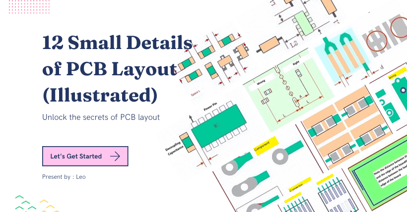
1. Spacing Between the Patches
Spacing between surface mount components is an essential consideration for engineers during the layout process. If the spacing is too small, it becomes challenging to apply solder paste and avoid soldering joint difficulties accurately.
The recommended distances are as follows:
For components of the same kind: ≥ 0.3mm
For components of different kinds: ≥ 0.13*h + 0.3mm (where h is the maximum height difference among neighboring elements)
For components that are manually placed: ≥ 1.5mm.
These suggestions are provided for reference and can be adjusted according to your company’s PCB process design specifications.
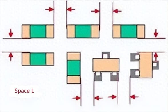
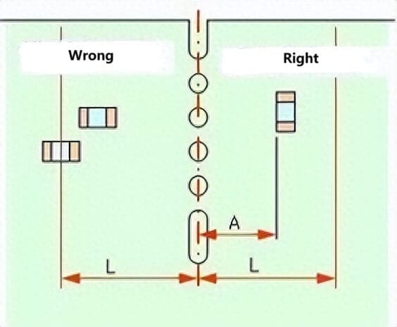
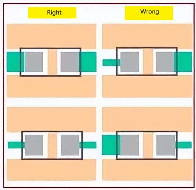
2. Distance Between Through-Hole Components and SMT
As shown in the above diagram, there should be a sufficient distance maintained between through-hole resistor components and surface mount components, with a recommended range of 1-3mm.
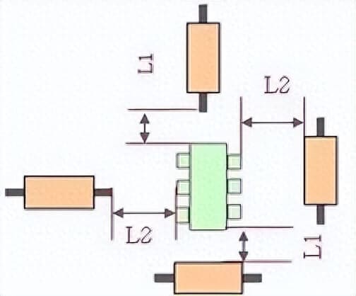
3. Placement of Decoupling Capacitors for ICs
A decoupling capacitor needs to be placed near the power ports of each IC. The placement should be as close as possible to the IC’s power port. When a chip has multiple power ports, a decoupling capacitor should be arranged near each port.
4. Guidelines for Placement Direction and Distance of Components at the PCB Board Edge
Due to the common use of panelization in PCB fabrication, components near the board edge must adhere to two conditions.
Firstly, they should be oriented parallel to the cutting direction (to ensure even mechanical stress distribution). For instance, if placed as shown on the left side of the diagram, differing forces on the two solder pads when breaking the panel could lead to detachment between the component and the solder pad.
Secondly, components must not be placed within a certain distance from the edge (to prevent damage during the board-cutting process).
5. Considerations for Connecting Adjacent Solder Pads
When connecting adjacent solder pads, it’s crucial to ensure that the connection is made outside to prevent inadvertent bridging and tangling. Additionally, pay close attention to the width of the copper trace in such scenarios.
6. If solder pads are situated within a copper pour area, thermal dissipation needs to be taken into consideration
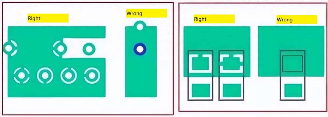
If solder pads are located within a copper pour area, the approach on the right should be employed to establish connections between the solder pads and the copper pour. Moreover, the decision to use either one or four wires to make the connection should be based on the magnitude of the current.
If the approach on the left is chosen, it can prove challenging during soldering or component removal for maintenance, as the temperature gets evenly dispersed through the copper pour, hindering proper soldering.
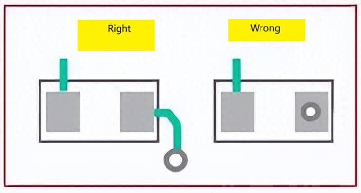
7. If the lead is smaller than the pad for through-hole components, the addition of a solder fillet (teardrop) is necessary
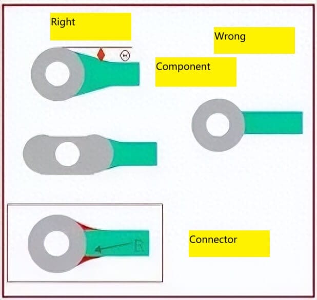
If the wire is smaller than the pad for through-hole components, the method on the right side of the diagram (adding a solder fillet or teardrop) should be employed.
Adding teardrops provides the following advantages:
- It prevents sudden signal line width reduction that can cause reflections, ensuring a smoother transition in the connection between traces and component pads.
- It addresses the issue of potential breakage in the connection between pads and traces due to impact.
- Incorporating teardrops also enhances the aesthetics of the PCB circuit board.
8. The width of leads on both sides of the component’s solder pad should be consistent
The width of leads on both sides of the component’s solder pad should be the same.
9. Ensure that unused pins on components are retained as solder pads and connected to the ground
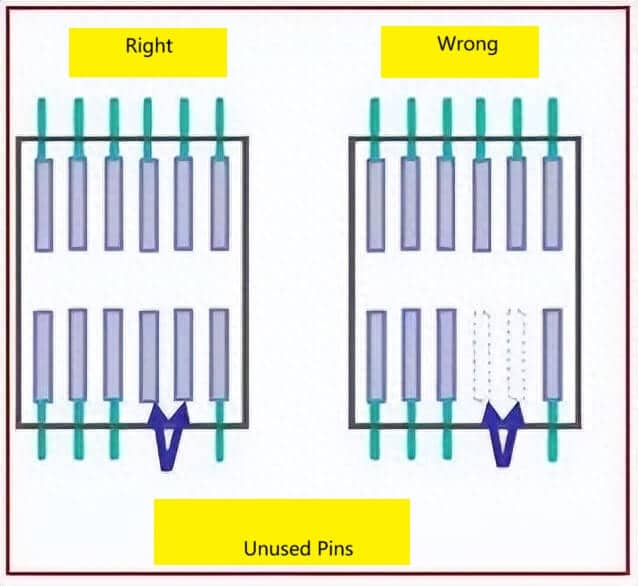
Be sure to retain solder pads for unused pins and connect them to the ground.
For example, in the diagram above, if there are two unused pins on a chip, although these pins are not functionally needed, they physically exist on the chip. Adopting the approach on the right side of the diagram—where the two pins are left hanging—can lead to potential interference. By adding solder pads and grounding them, interference can be effectively mitigated.
10. It’s advisable to avoid drilling through holes directly on solder pads
It’s important to avoid placing through-holes directly on solder pads, as this can lead to issues like solder bridging and insufficient solder joints.
11. Pay attention to the distance between wires or components and the board edge

It’s important to ensure that leads or components are not positioned too close to the board edge, especially in the case of single-sided boards. Single-sided boards are often made of materials like paper-based substrates, which can be fragile and prone to breakage under stress. Placing traces or components near the edge could lead to structural vulnerabilities.
12. It’s essential to consider the ambient temperature and keep electrolytic capacitors away from heat sources
Firstly, it’s crucial to assess whether the ambient temperature meets the requirements for electrolytic capacitors. Secondly, it’s advisable to position the capacitors as far away as possible from areas generating heat to prevent the liquid electrolyte inside the electrolytic capacitors from drying out.
Related:

Disclaimer: This account maintains a neutral stance on all original and reposted articles, and the views expressed therein. The articles shared are solely intended for reader learning and exchange. Copyright for articles, images, and other content remains with the original authors. If there is any infringement, please contact us for removal.