
NAND Flash Technology #
Embedded developers often encounter NAND flash-related storage devices. There are several characteristics regarding NAND flash:
- Encoding bits using varying voltage levels.
- All bits have an initial value of 1.
- Utilizing PROGRAM and ERASE operations.
- PROGRAM action sets a bit’s value to 0. The smallest execution unit is a Page.
- ERASE action sets a bit’s value to 1. The smallest execution unit is a Block (a Block contains multiple Pages).

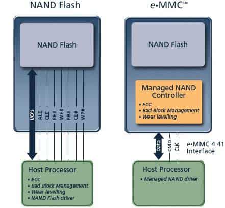
Recently, commonly seen eMMC (half-duplex), eMCP (half-duplex), and UFS (full-duplex) have a controller added to NAND flash for ECC, bad block management, and even write distribution. This helps in avoiding performance issues caused by filesystems (e.g., UBIFS, yaffs2, …) handling these tasks. NAND flash with such controllers is generally referred to as managed NAND flash, as shown in the diagram below:
NAND flash chips (The Difference between SLC, MLC, TLC, QLC, and PLC) are primarily divided into SLC, MLC, and TLC categories. The difference lies in how many bits each NAND Flash cell can store: SLC can store 1 bit, MLC can store 2 bits, and TLC can store 3 bits.
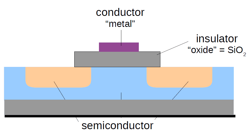
At first glance, it might seem odd that TLC, which can store more bits, is cheaper. To understand this, we need to delve into the operation principles of NAND flash. NAND flash primarily uses a floating gate to store electrons, surrounded by an insulator layer to protect it. Therefore, each time a PROGRAM or ERASE operation is performed, specific voltages are applied to create an electric field that forces electrons to pass through the insulator and enter or leave the floating gate. However, each passage through the insulator causes damage to it, and after a certain point, it loses its insulating ability, preventing the floating gate from retaining electrons.

In view of the above logic, the more frequent access to the floating gate will lead to a shorter lifespan. So if a cell stores more data (bits), its lifespan will be reduced due to frequent access.
The diagram below shows a comparison of flash type:
| Flash type | SLC, Single Level Cell (1 bit) | MLC, Multilevel Cell (2 bits) | TLC, Triple Level Cell (3 bits) |
| Bits per cell | 1 | 2 | 3 |
| Program/Erase cycles | Generally, 100,000 write-erase cycles | Anywhere from 3000 to 15000 write erase cycles | Anywhere from 1000 to 5000 write/erase cycles |
| Erase time | Erase time: 1.5-2 ms | Erase time: 2.5-3.5ms | Erase time: 4-5ms |
| Operation scenario | Industrial | Commercial | Commercial |
The Emergence of pSLC #
Over the past few years, a type of flash memory called “pSLC” (pseudo-SLC) has been gradually gaining popularity. pSLC is based on the MLC flash type but stores only 1 bit per cell instead of 2 bits. Since it stores only one bit per cell, like SLC, but is not truly SLC, it is called “pSLC” (pseudo-SLC).
According to the above principle, if you switch from MLC to pSLC, the storage capacity is halved. For example, 8G MLC becomes 4G pSLC. Because it reduces access to the floating gate, pSLC can significantly increase the lifespan compared to MLC in terms of read and write operations.
The purpose of “pSLC” (pseudo-SLC) is to achieve “close to” SLC-level read and write lifespan and access performance at the price of halving the storage space. pSLC is controlled by the NAND flash controller, so not every manufacturer supports it. Before using it, you need to ensure that the storage device is managed by NAND flash and that the controller on top of it supports this mode.
The diagram below shows a comparison chart with the addition of the pSLC flash type:
| Flash type | SLC, Single Level Cell (1 bit) | pSLC, pseudo Single Level Cell (1 bit) | MLC, Multilevel Cell (2 bits) |
| Bits per cell | 1 | 1 | 2 |
| Program/Erase cycles | Generally, 100,000 write-erase cycles | Anywhere from 30000 to 50000 write erase cycles | Anywhere from 3000 to 15000 write erase cycles |
| Erase time | Erase time: 1.5-2 ms | N/A | Erase time: 2.5-3.5ms |
| Operation scenario | Industrial | Industrial | Commercial |
Bonus Chart #
| NAND Flash Type | Feature | P/E Cycle | W/R Speed | Price | |
|---|---|---|---|---|---|
| 2D NAND | SLC | Single-Level Cell | 60,000-100,000 | Best | Expensive |
| 2D NAND | pSLC | Pseudo SLC | 20,000-50,000 | Great | Between SLC & MLC |
| 2D NAND | MLC | Multi-Level Cell | 3,000 | Good | Cheap |
| 3D NAND | 3D pSLC | 3D Pseudo SLC | 20,000-50,000 | Great | Close to MLC |
| 3D NAND | 3D pMLC | 3D Pseudo MLC | 3,000 | Good | Between 3D pSLC & 3D TLC |
| 3D NAND | 3D TLC | 3D Triple-Level Cell | 1,000-3,000 | Worst | Lowest |

Related:


