
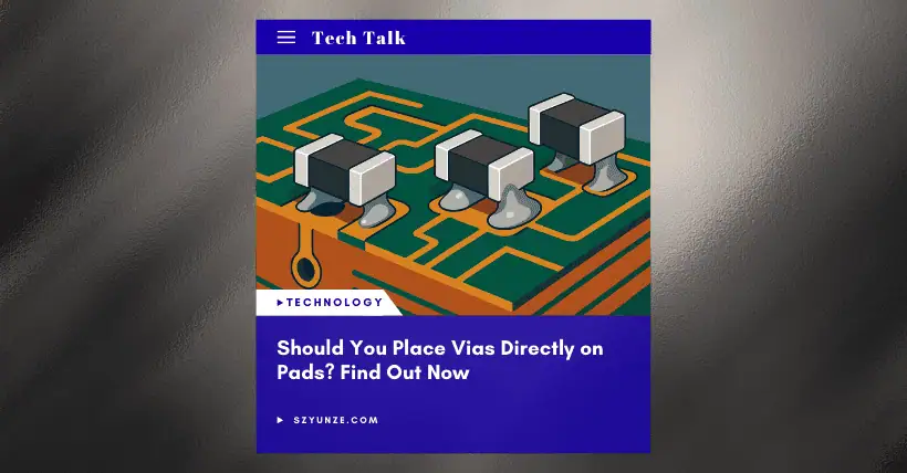
In PCB design, the topic of “placing vias directly on pads” is frequently discussed by both beginners and experienced engineers. Recently, some learners have asked:
Can vias actually be placed directly on pads? What are the consequences of such a design?
Today, let’s clarify everything with two key principles!
01|Theoretically feasible, practically not recommended
Let’s start with two fundamental points:
First: Theoretically, placing a via directly on a pad minimizes lead inductance, so it is possible.
For certain high-speed or high-frequency designs, this seems to be the “optimal connection path.”
But the problem lies in the second point—
Second: From a soldering process perspective, this approach can lead to serious issues.
Especially when the via isn’t properly filled, it can cause solder paste to leak into the hole, leading to weak solder joints or component lifting.
02|Common problems with via-in-pad: solder leakage & tombstoning
Solder leakage
If the via is not completely sealed, solder paste may flow down through the via during reflow soldering, resulting in insufficient solder on the pad and ultimately weak or failed solder joints.
Tombstone Effect
When the two ends of an SMD component are heated unevenly, one side’s solder paste melts first due to solder leakage or uneven heat conduction. The component may then “stand up” due to the unbalanced force.
This is especially common with chip resistors and capacitors and is one of the typical defects in SMT assembly.
03|Technical terms explained: Lead inductance & Tombstone Effect
Lead inductance
In high-frequency circuits, conductors themselves exhibit inductive reactance. Especially the “lead section” between a via and a pad can easily form parasitic inductance, which negatively impacts high-speed signals or power integrity.
So, theoretically, the shorter, the better.
Tombstone Effect
Also known as the “Manhattan Effect,” it often occurs during the soldering of SMD components. Due to uneven force on both ends, one side of the component lifts, resulting in a failed solder joint.
04|Recommended approach: offset via from pad
Combining theory and practice, we recommend the following design:
Move the via away from the pad and connect it with a short trace.
Advantages:
- Maintains low lead inductance
- Avoids manufacturing defects
- Improves soldering yield
Designing is not just about drawing traces—it’s a comprehensive art that balances signal integrity, electrical performance, and manufacturability.
Never underestimate the placement of a single via; it can determine whether your design can be successfully assembled and shipped!

Disclaimer:
- This channel does not make any representations or warranties regarding the availability, accuracy, timeliness, effectiveness, or completeness of any information posted. It hereby disclaims any liability or consequences arising from the use of the information.
- This channel is non-commercial and non-profit. The re-posted content does not signify endorsement of its views or responsibility for its authenticity. It does not intend to constitute any other guidance. This channel is not liable for any inaccuracies or errors in the re-posted or published information, directly or indirectly.
- Some data, materials, text, images, etc., used in this channel are sourced from the internet, and all reposts are duly credited to their sources. If you discover any work that infringes on your intellectual property rights or personal legal interests, please contact us, and we will promptly modify or remove it.