
On the stage of semiconductor manufacturing, silicon wafers undergo a transformation from crystal slicing to functional devices. The sliced wafers bear sharp edges, damaged surface layers, internal stress, and oxygen impurities—issues that directly affect chip performance and yield. To address this, three critical processes—chamfering, grinding, and heat treatment—work together like precision sculpting tools to shape silicon wafers that meet stringent requirements.
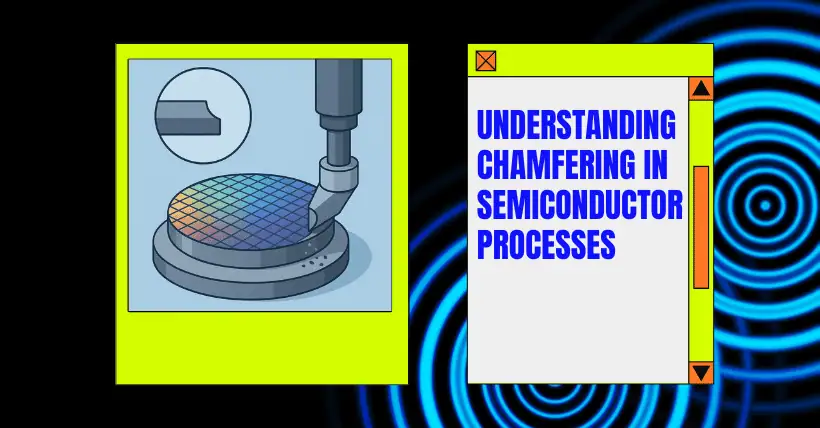
The sharpness and microscopic defects at the wafer’s edges are potential “weak zones,” prone to chipping during subsequent processes. Chamfering is designed to resolve this.
A high-speed rotating diamond wheel (6000–8000 r/min) precisely grinds the wafer edge. Through multi-stage grinding (e.g., from coarse 800# to fine 3000#), it forms a smooth R-type or T-type rounded contour. This not only eliminates points of physical stress concentration but also significantly enhances the wafer’s mechanical strength.
The process relies on precision control: wafer centering error must be under microns, and the distance L between the grinding wheel and wafer must meet L < R – d (R = wafer radius, d = offset); any deviation can cause uneven chamfering or residual sharp edges. For special wafers with reference flats, cam-driven systems replace conventional circular motion, ensuring that every irregular edge is uniformly ground to an ultra-smooth state with Ra < 0.04μm.
After slicing, the wafer surface retains a damage layer of about 30μm (lattice distortion, scratches). Grinding removes this layer and lays the foundation for polishing. Double-sided grinding machines take the lead in this phase: upper and lower high-hardness grinding plates rotate in opposite directions while holding the wafer, embedded in a planetary gear system, in a complex composite motion. The key to grinding lies in the slurry—precisely formulated from SiC particles, water, and a weakly alkaline additive in a 10:20:4 ratio. SiC abrasives (particle size 10–14μm) handle the cutting; surfactants in the additive prevent particle agglomeration and react with the silicon surface to create a removable loose oxide layer; water ensures cooling, lubrication, and chip removal.
Process parameters act like the conductor of a symphony:
Concentration: Grinding rate rises then falls with SiC concentration; the peak must be optimized experimentally.
Pressure: Increasing pressure boosts grinding rate, but must be staged to prevent wafer breakage.
Speed: Higher speeds improve efficiency, but must be balanced with pressure to avoid surface defects like chipping and cracks.
As a result, wafer thickness variation (TTV) improves from tens of microns to <5μm, and surface flatness undergoes a qualitative leap.
Heat Treatment: Taming the “Rebellious” Oxygen Atoms
Oxygen impurities in Czochralski-grown wafers (concentration up to 10¹⁸/cm³) are a key cause of resistivity instability. High-temperature annealing (650°C ± 20°C) becomes the critical solution. In a quartz tube furnace filled with nitrogen or argon, wafers undergo a steady 30–40 minute heat treatment. This process targets two donor effects of oxygen atoms:
Thermal donors (formed at 300–550°C): Dispersed oxygen atoms cause large fluctuations in resistivity; annealing at 650°C localizes and eliminates them.
New donors (formed at 500–800°C): Larger oxygen-silicon complexes, more stable and less impactful, are usually retained.
Interestingly, during cooling, a moderate amount of oxygen forms oxygen precipitates (SiO₂ particles). This “defect” is dual-natured: excess leads to wafer warping, but trace amounts can absorb metallic impurities and enhance mechanical strength—becoming an unexpected “guardian.”
Conclusion
Chamfering gives the wafer a resilient edge, grinding provides a mirror-smooth foundation, and heat treatment stabilizes its electrical properties at the atomic level. The synergy of these three precision processes transforms a fragile, rough-cut silicon wafer into a flawless stage for housing trillions of transistors. In the nanoscale world of semiconductors, these seemingly traditional techniques lay the unshakable groundwork for the continuation of Moore’s Law.
Related:

Disclaimer: This article is created by the original author. The content of the article represents their personal opinions. Our reposting is only for sharing and discussion purposes and does not imply our endorsement or agreement. If you have any objections, please get in touch with us through the provided channels.