
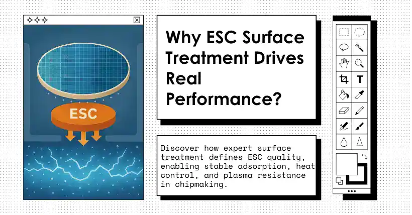
In semiconductor manufacturing equipment, the Electrostatic Chuck (ESC) performs multiple functions including wafer adsorption and fixation, heat conduction, and uniform electrostatic discharge. The industry often categorizes ESC applications into “high-end” and “low-end” types, but what truly determines their performance ceiling is not the external structure or base material formula, but a more “hidden” factor—the surface treatment process.
01
Why Is Surface Treatment Considered The Performance Watershed For ESC?
One of the core functions of an ESC is to stably adsorb wafers under extreme conditions such as high vacuum, strong plasma, and a wide temperature range (-20°C to 200°C). Without professional surface treatment, the ESC may encounter the following issues:
- Plasma corrosion and metal ion contamination
In etching or CVD environments, unprotected ceramic surfaces are prone to plasma erosion, leading to particle shedding or metal ion release, which can cause wafer contamination. - Uneven thermal conductivity and warping deformation
If the surface is rough or poorly treated, contact between the wafer and the ESC becomes uneven, hindering thermal conduction and affecting CD uniformity. - Unstable electrostatic adsorption
If the surface’s insulating or conductive properties are not well controlled, it may lead to local arcing, insufficient adsorption force, or excessive adsorption, affecting wafer processing yield.
High-end ESC surfaces often adopt composite multilayer structural designs. By precisely regulating the coating of functional areas, they achieve true high-performance integration.
02
Mainstream Surface Coating Technologies For High-End ESCs
The following are common surface treatment technologies currently used in high-end ESCs:
- Fluoropolymer (PTFE/PFA) non-adhesive coatings
With low surface free energy, these coatings prevent adhesion of focus rings or photoresist residues, making them suitable for low-temperature process environments. - DLC (Diamond-Like Carbon) coatings
Featuring high hardness, plasma resistance, and low friction coefficient, these are ideal for corrosion and particle-shedding resistance in etching equipment. - PVD conductive ceramic films such as CrSiN/TiN
These can form stable conductive paths in specific areas to control uniform surface charge discharge and prevent local charge buildup. - Composite thermal conductive coatings
For example, a diamond powder + fluoropolymer mixed system, which combines thermal conduction with non-adhesive properties, suitable for high-precision thermal control ESCs.
If ESC coating is needed, you may contact Tom for recommendations on professional coating suppliers.
Related:
- Understanding Chamfering in Semiconductor Processes
- How to Fix Wafer Ripple Defects After Surface Cleaning?
- Best Way to Clean Silicon Wafers for Top Performance
- Wafer Cleaning Expiry Time: What You Must Know
- Function of HCl in Copper Plating of Semiconductor Wafers

Disclaimer:
- This channel does not make any representations or warranties regarding the availability, accuracy, timeliness, effectiveness, or completeness of any information posted. It hereby disclaims any liability or consequences arising from the use of the information.
- This channel is non-commercial and non-profit. The re-posted content does not signify endorsement of its views or responsibility for its authenticity. It does not intend to constitute any other guidance. This channel is not liable for any inaccuracies or errors in the re-posted or published information, directly or indirectly.
- Some data, materials, text, images, etc., used in this channel are sourced from the internet, and all reposts are duly credited to their sources. If you discover any work that infringes on your intellectual property rights or personal legal interests, please contact us, and we will promptly modify or remove it.