
✅ I. What is Chip Backend Design?
Chip backend design, also known as physical design, begins with the gate-level netlist derived from the logical (frontend) design and gradually implements it into a manufacturable chip layout. Its essential task is to “land” the circuit: accurately and securely placing the functional logic onto the silicon while meeting various physical constraints such as timing, power, area, and power consumption.
Analogy: Frontend design is like “writing a script and setting up character relationships”, while backend design is the “director turning the script into a movie”, needing not only to faithfully reproduce the plot, but also to consider real-world constraints such as filming locations, actor scheduling, and lighting arrangements.
✅ II. Complete Backend Design Flow and Major Tools
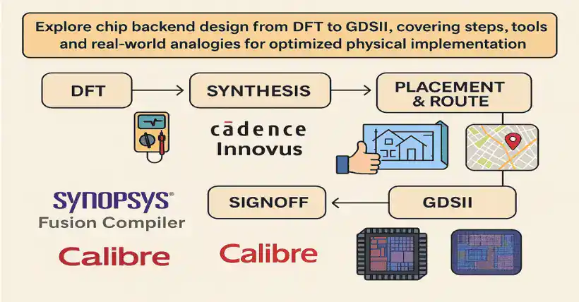
- DFT (Design for Test)
Purpose: Reserve test structures during chip design to facilitate future mass production testing and improve yield.
Key tasks:
- Insert scan chains to control/observe register states.
- Add memory test circuits (MBIST).
- Layout test pins (JTAG, BSCAN).
Common tools:
- Synopsys:
- DFT Compiler (scan chain insertion)
- TetraMAX (ATPG pattern generation)
- Mentor Tessent:
- MBISTArchitect (memory test structures)
- TestKompress (test vector compression)
- Cadence Modus (integrates DFT, BIST, and ATPG)
Analogy: DFT is like installing a “self-check system” before car manufacturing, making future maintenance and servicing easier.
- Floorplanning
Purpose: Determine the rough location of each module (IP, RAM, IO, etc.) on the chip.
Key tasks:
- Define chip boundaries and IO placement.
- Determine core area, macro blocks, channels, etc.
- Set up power planning.
Common tools:
- Cadence Innovus (formerly Encounter)
- Synopsys IC Compiler II
- Mentor Olympus-SoC
Analogy: Floorplanning is like urban planning, reasonably arranging houses, schools, hospitals, and roads on a map.
- Placement
Purpose: Place tens of thousands of standard cells (logic gates, flip-flops, etc.) onto the chip core area based on the netlist.
Key tasks:
- Optimize cell placement to reduce wire length.
- Pre-optimize congestion and power consumption.
- Reserve whitespace for clock trees and routing.
Common tools:
- Cadence Innovus
- Synopsys IC Compiler II
- Siemens Aprisa (Mentor)
Analogy: Like assigning actual locations for buildings in a city, considering space, traffic, and resource supply.
- CTS (Clock Tree Synthesis)
Purpose: Build a symmetrical, balanced, and low-skew clock distribution network to ensure synchronous triggering of all registers.
Key tasks:
- Minimize clock skew.
- Control insertion delay.
- Support complex designs like multi-domain clocks and multi-source synchronization.
Common tools:
- Cadence Innovus (CT-Gen engine)
- Synopsys IC Compiler II (Clock Tree Compiler)
- Siemens Olympus-CTS
Analogy: CTS is like laying the main water pipeline network for a city, ensuring balanced water pressure everywhere.
- Routing
Purpose: Establish actual metal connections for all logical links, converting the netlist into layout.
Key tasks:
- Accurate routing (adhering to width, spacing, and metal layer rules).
- Optimize congestion and crosstalk.
- Support multilayer routing and efficient via usage.
Common tools:
- Cadence Innovus
- Synopsys IC Compiler II
- Siemens Aprisa / Mentor Nitro-SoC
Analogy: Like laying roads and power lines in a city, connecting all buildings through communication and electricity lines.
- Parasitic Extraction
Purpose: Extract parasitic effects such as wire capacitance and resistance for accurate timing simulation and signal integrity analysis.
Key tasks:
- RC network modeling (R: resistance, C: capacitance).
- Consider power noise and coupling effects.
- Provide post-simulation files like SDF/SPEF.
Common tools:
- Synopsys StarRC
- Cadence Quantus
- Mentor Calibre xRC
Analogy: Measuring electrical performance of wired cables to verify voltage and current reliability.
- Sign-off STA (Static Timing Analysis)
Purpose: Combine parasitic parameters to perform full-chip static timing analysis and confirm there are no violations.
Key tasks:
- Check setup/hold violations.
- Multi-mode multi-corner (MMMC) sign-off.
- Support DVFS (Dynamic Voltage and Frequency Scaling) scenarios.
Common tools:
- Synopsys PrimeTime
- Cadence Tempus
- Siemens Aegis STA
- Physical Verification (DRC/LVS)
Purpose: Ensure the layout meets manufacturing process requirements and that logical and physical designs are consistent.
Key tasks:
- DRC (Design Rule Check): Check line width, spacing, vias, etc. for process compliance.
- LVS (Layout vs. Schematic): Confirm that layout matches gate-level netlist functionality.
- Support graphical debugging.
Common tools:
- Mentor Calibre (industry standard)
- Synopsys Hercules
- Cadence Pegasus / Assura / Dracula
Analogy: Like construction inspection—checking if wiring and circuits comply with standards and match blueprints.
- Post-layout Simulation
Purpose: Verify whether routing and parasitic effects affect functional timing, ensuring the “real circuit” still works correctly.
Key tasks:
- Use SDF files to apply real delays.
- Run Verilog/VHDL simulations.
- Check whether waveform still meets expectations.
Simulation tools: Same as pre-simulation
- Modelsim (Mentor)
- VCS (Synopsys)
- NC-Verilog (Cadence)
- GDSII Generation and Tape-out Delivery
Purpose: Output final layout in GDSII format and hand it off to the foundry for manufacturing.
Key tasks:
- Package GDS files (with all hierarchy and layers).
- Provide process parameter files (.lef/.lib/.tf).
- Coordinate tape-out schedule and mask preparation with foundry.
✅ III. Backend Tool Summary Table
| Design Stage | Tools & Vendors |
|---|---|
| DFT | Synopsys (DFT Compiler, TetraMAX), Mentor Tessent, Cadence Modus |
| Floorplanning | Cadence Innovus, Synopsys ICC II |
| Placement | Same as above |
| CTS | Synopsys Clock Tree Compiler, Cadence CT-Gen |
| Routing | Synopsys ICC II, Cadence Innovus |
| Parasitic Extraction | StarRC (Synopsys), Calibre xRC (Mentor) |
| STA | PrimeTime (Synopsys), Tempus (Cadence) |
| DRC/LVS | Calibre (Mentor), Pegasus (Cadence) |
| Post-simulation | VCS / Modelsim / NC-Verilog |
| Final Layout Output | GDSII (produced by all physical design tools) |
✅ IV. Summary
Chip backend design is a crucial bridge from “logic” to “physical”, requiring collaboration among many tools to complete key steps such as placement, routing, clock distribution, and verification, ultimately delivering high-quality layout files for fabrication. Each stage uses specialized tools working together to build a complete physical implementation system.
Related:

Disclaimer:
- This channel does not make any representations or warranties regarding the availability, accuracy, timeliness, effectiveness, or completeness of any information posted. It hereby disclaims any liability or consequences arising from the use of the information.
- This channel is non-commercial and non-profit. The re-posted content does not signify endorsement of its views or responsibility for its authenticity. It does not intend to constitute any other guidance. This channel is not liable for any inaccuracies or errors in the re-posted or published information, directly or indirectly.
- Some data, materials, text, images, etc., used in this channel are sourced from the internet, and all reposts are duly credited to their sources. If you discover any work that infringes on your intellectual property rights or personal legal interests, please contact us, and we will promptly modify or remove it.