
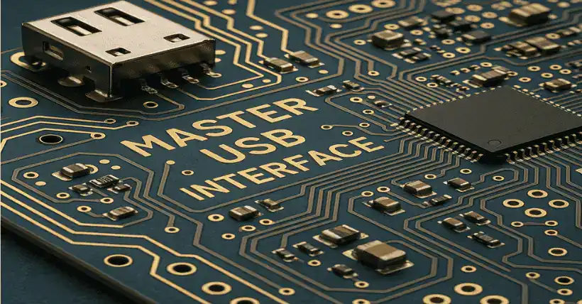
USB Interface: From Basics to the Cutting Edge
As the core interface connecting devices and hosts, USB (Universal Serial Bus) has evolved over years of iteration—from the low-speed USB 1.0 to the high-speed USB 3.1 era with 10Gbps transmission and 100W power delivery capability.
With its reversible plug and high compatibility, the Type-C connector has become the mainstream choice for mobile devices and laptops. However, high-speed transmission places higher demands on PCB design. How can signal integrity be balanced with EMI performance? This article combines practical experience to detail the key points of USB interface design!
I. Layout Design: Details Determine Success
✅ Connector Position and ESD Protection
• Near board edge: USB connectors should extend 3–5mm beyond the board edge for easy plugging.
• ESD and common mode choke layout: ESD devices should be placed right next to the USB port, ≤1.5mm away, followed by common mode chokes and RC filter circuits.
Note: Maintain spacing between ESD devices and the USB shell to avoid damage during reflow soldering.
✅ Protection Ground Isolation Design of Positioning Posts
Ground handling: If positioning posts on both sides of the USB are connected to protection ground (PGND), they must be at least 2mm from system GND and connected via ferrite beads.
Add ground vias: Densely place vias in the PGND region to ensure low-impedance grounding and suppress electrostatic interference.
II. Differential Pair Routing: Impedance Control and EMI Suppression
- Differential Pair and Surrounding Ground Impedance Requirements
USB 2.0 requires a differential impedance of 90Ω±10%, while USB 3.0/3.1 must strictly maintain 90Ω. Surrounding ground: Copper should be placed on both sides of the differential pair, with spacing ≤3 times the trace width to absorb high-frequency noise.
- Routing Layer and Reference Plane
Prefer inner-layer routing: Reduces external electromagnetic radiation and ensures a solid ground plane below.
Avoid: Do not cross split planes to prevent impedance discontinuity and noise coupling.
- Via Optimization and Return Path
Minimize layer changes: Vias add parasitic capacitance; limit the number of layer changes to ≤2.
Add return ground vias: For each layer change, place a pair of ground vias next to the differential vias to provide a low-impedance return path and reduce signal integrity risks.
III. Advanced Techniques for High-Speed USB 3.1 Design
✅ Length Matching and Spacing Control
Internal matching of differential pairs: Length mismatch ≤5mil; ≤2mil is recommended for USB 3.1.
• Pair spacing: Keep ≥4 times the trace width to prevent crosstalk.
✅ Power and Signal Isolation
Dedicated power layer: Allocate independent power regions for VBUS (5V/12V/20V) to avoid overlap with high-speed signal layers.
Filter capacitor layout: Place 10μF + 0.1μF capacitors near the VBUS pin to filter high-frequency noise.
IV. Special Design Points for Type-C Interface
✅ CC Pins and PD Protocol
CC pin routing: Impedance should match (90Ω), and length should match other differential pairs to ensure protocol communication stability.
• VBUS path: High current paths (e.g., 20V@5A) should be widened to over 80mil and use grid copper to reduce thermal rise.
✅ Symmetrical Layout Design for Reversible Insertion Compatibility
The 24 pins of Type-C should be symmetrically laid out to avoid signal path differences due to plug orientation.
V. Common Issues and Solutions
✅ Signal Ringing
Cause: Impedance discontinuity or incomplete return path.
• Solution: Optimize number of ground vias next to signal vias; check for complete reference planes.
✅ EMI Test Failure
Cause: Differential pair exposed on outer layer or insufficient ground shielding.
• Solution: Route on inner layers with ground shielding on both sides; add shielding can at connector.
VI. Conclusion: Standardized Design for Reliable Implementation
Layout comes first: Connector position, ESD protection, and ground isolation are the basics.
Impedance is king: Strict impedance matching, inner-layer routing, and ground shielding reduce EMI.
Details determine performance: Via return paths and symmetrical Type-C design are key for high-speed reliability.
By following the above design principles (as shown in the diagrams), even USB 3.1 and Type-C interfaces can achieve stable transmission and high reliability with ease!
Related:

Disclaimer:
- This channel does not make any representations or warranties regarding the availability, accuracy, timeliness, effectiveness, or completeness of any information posted. It hereby disclaims any liability or consequences arising from the use of the information.
- This channel is non-commercial and non-profit. The re-posted content does not signify endorsement of its views or responsibility for its authenticity. It does not intend to constitute any other guidance. This channel is not liable for any inaccuracies or errors in the re-posted or published information, directly or indirectly.
- Some data, materials, text, images, etc., used in this channel are sourced from the internet, and all reposts are duly credited to their sources. If you discover any work that infringes on your intellectual property rights or personal legal interests, please contact us, and we will promptly modify or remove it.