
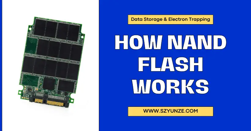
NAND flash memory arranges cells in series to achieve high-density storage, prioritizing write/erase speed over direct addressing.
Flash memory stores data using floating-gate transistors in a grid. During the write process, electrons are captured via quantum tunneling, altering the cell voltage. Erase operations use block-level voltage pulses to reset the charge. Due to the insulating oxide layer, data is preserved even during power loss, though repeated writes can degrade the performance of the cells.
01
How do floating-gate transistors store data?
The floating gate traps electrons between the oxide layers, thereby changing the transistor’s threshold voltage. This binary state (0/1) is read by sensing current. Unlike DRAM, the charge remains intact without needing refresh cycles.
The core of each flash cell is a MOSFET, with an additional floating gate sandwiched between the control gate and the substrate. During programming, a high voltage (15-20V) forces electrons through the Fowler-Nordheim tunneling effect across the tunnel oxide. These trapped electrons raise the transistor’s threshold voltage, which can be detected during reading. Essentially, this is like filling a bucket (floating gate) with water: the water doesn’t leak unless forcibly emptied. Modern 3D NAND vertically stacks cells and uses Charge-Trap Flash (CTF) to reduce electron leakage. However, what happens if the oxide degrades? Similar to a rusty pipe, a damaged insulating layer causes electron leakage, leading to data corruption. Manufacturers use error correction codes (ECC) and stricter voltage margins to address this issue.
02
What is the difference between NAND and NOR flash architectures?
NOR flash uses parallel cells for random access, making it ideal for firmware. NAND flash arranges cells in series for high-density storage, prioritizing write/erase speed rather than direct addressing.
NOR’s parallel structure allows for byte-level reads, making it behave like traditional RAM but with non-volatility. However, the erase block is large (64-128KB), and the write speed is slow. In contrast, NAND links 32-64 transistors in series, enabling page-level operations (4-16KB) and cheaper high-density designs. Think of NOR as a library where you can pick any book (byte) directly, whereas NAND is like a conveyor belt—you must process an entire box (page) at once. Technically, NAND achieves higher durability (100K cycles, compared to NOR’s 10K) due to its simpler cell structure. For SSDs, manufacturers prefer 3D TLC NAND because it offers cost advantages per GB, even though the write speed is slower. One key trade-off: NOR’s latency is in microseconds, whereas NAND’s random access latency is in milliseconds.
| Feature | Nand | Nor |
|---|---|---|
| Access Type | Sequential | Random |
| Density | High (1Tb+) | Low (Max 2Gb) |
| Device | Storage drive | BIOS/UEFI Firmware |
03
How are data write and erase operations carried out?
Write operations inject electrons via tunneling, while erase operations use hot carrier injection to release the charge. Both require high-voltage circuits, which stress the oxide layer over time.
During programming, a voltage difference (7-10V on the control gate and 0V on the substrate) creates a strong enough electric field to push electrons through the tunnel oxide. During erase, a 20V substrate bias is applied to reverse this process and pull the electrons back. The problem is that erasure affects the entire block (256KB-4MB), not just a single byte. Why? Because applying such high voltages to each cell would require impractical circuitry. It’s like repainting an entire wall (block) rather than patching up scattered bricks (bytes). SSDs alleviate the erasure overhead through over-provisioning—keeping extra cells to distribute wear. However, excessive writes still generate electron traps in the oxide, permanently raising the cell’s threshold voltage.
04
What role does error correction play in flash memory lifespan?
ECC algorithms can detect/correct bit errors caused by charge leakage or write interference. Advanced schemes like LDPC can compensate for issues in aging cells but introduce added latency.
Since flash cells endure programming/erase cycles, oxide wear increases the bit error rate (BER). SLC (1 bit/cell) may withstand 100K cycles using basic BCH codes, while TLC (3 bits/cell) requires robust LDPC codes for 10K cycles. Think of ECC as spell check for data—small errors are automatically fixed, but too many spelling mistakes require rewriting the entire paragraph (data retry). Technically, LDPC uses probabilistic models to guess the original charge, but this requires more computational power. Disabling ECC for speed (e.g., in DIY SSD projects) can lead to silent data corruption. Beyond software, hardware techniques like cross-chip RAID redundancy can also help. Did you know? A 1% BER in QLC NAND can spike to 25% after three years—so consumer SSDs hide this with aggressive ECC.
| ECC | Corrected Bit Count | Example |
|---|---|---|
| Biosafety Information Exchange Center | 4-24/KB | SLC/MLC Enterprise |
| Low-Density Parity Check Code | 40-100/KB | TLC/QLC Consumer |
05
How does wear leveling extend flash memory lifespan?
Wear leveling technology uses firmware mapping to evenly distribute write operations across blocks. Dynamic and static methods prevent “hot spots” from prematurely wearing out cells.
The flash controller tracks the erase count of each block via a logical-to-physical address table. Dynamic wear leveling redirects new writes to less-used blocks, while static wear leveling periodically moves stale data. It’s like rotating car tires—uniform wear maximizes total mileage. For example, a 1TB SSD with 3K endurance and 10% over-provisioning can handle 3.3PB of writes, equivalent to writing 45GB daily for 20 years. However, due to write amplification caused by small random writes, the controller typically fails earlier. Pro tip: Use the TRIM command to mark deleted files, allowing the controller to pre-erase blocks during idle time. However, wear leveling can’t address the inherent cell performance degradation—eventually, all NAND becomes unreliable.
06
Why does the performance of flash memory cells degrade over time?
Repeated tunneling effects stress the oxide layer, forming electron traps that impede charge movement. Accumulated damage increases leakage current until the cell can no longer maintain the required voltage level.
Each programming/erase cycle creates defects in the silicon lattice. Initially, ECC can mask these errors, but eventually, the traps accumulate, causing the cells to become “sticky”—they either fail to fully charge (programming interference) or leak too quickly (data retention failure). It’s like a garden hose: small cracks lead to tiny leaks (correctable errors), but a complete break requires replacement (bad block). Technically, the data retention time in worn QLC decreases from 10 years (new SLC) to just months. High-temperature environments accelerate this process—data centers actively cool SSDs to below 15°C.

Disclaimer:
- This channel does not make any representations or warranties regarding the availability, accuracy, timeliness, effectiveness, or completeness of any information posted. It hereby disclaims any liability or consequences arising from the use of the information.
- This channel is non-commercial and non-profit. The re-posted content does not signify endorsement of its views or responsibility for its authenticity. It does not intend to constitute any other guidance. This channel is not liable for any inaccuracies or errors in the re-posted or published information, directly or indirectly.
- Some data, materials, text, images, etc., used in this channel are sourced from the internet, and all reposts are duly credited to their sources. If you discover any work that infringes on your intellectual property rights or personal legal interests, please contact us, and we will promptly modify or remove it.