
According to industry sources, Samsung Electronics is researching various bonding technologies for next-generation HBM, including fluxless bonding.
Since the beginning of this year, Samsung Electronics has been conducting preliminary evaluations of fluxless bonding technology in collaboration with major overseas partners.
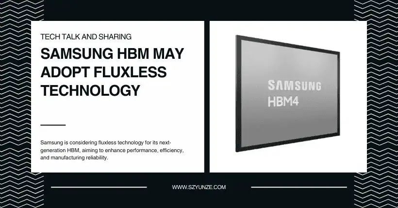
This technology will be applied to HBM4 (sixth generation), with the goal of completing evaluations by the end of this year.
Currently, Samsung Electronics uses NCF (Non-Conductive Film) as a post-process technology for HBM manufacturing.
HBM is a memory semiconductor that enhances data processing performance by vertically stacking multiple DRAMs. It drills microscopic holes into each DRAM using TSV (Through-Silicon Via) and electrically connects these holes. To link individual DRAMs, tiny protrusions called microbumps are used.
Samsung Electronics has traditionally employed a TC bonding process, in which NCF is inserted between each stacked DRAM and then thermocompressed from above. Under high temperatures, NCF melts, facilitating the connection between bumps and securing the chips together.
Fluxless technology is mainly applied in MR-MUF (Mass Reflow-Molded Underfill). MR-MUF does not use film but instead employs liquid EMC (Epoxy Molding Compound), a mixture of epoxy resin and inorganic silica.
In MR-MUF, each DRAM is temporarily thermocompressed during stacking. Once fully stacked, the bonding process is completed through heating (reflow soldering).
Afterward, EMC is injected between the chips without gaps. EMC functions as an “underfill” that supports the chips and prevents external contamination.
In the existing MR-MUF process, a substance called flux is applied to remove the oxidation layer on the bumps, which is then washed away.
However, as the number of I/O terminals in HBM4 has doubled to 2,024 compared to previous generations, and DRAM stack layers have increased, the spacing between bumps has become narrower.
In this situation, flux may not be completely removed, potentially compromising chip reliability.
To address this, the semiconductor industry has proposed fluxless soldering solutions.
Although equipment manufacturers have different approaches to fluxless technology, the core principle is to remove the oxidation layer around solder balls without using flux.
Related:

Disclaimer:
- This channel does not make any representations or warranties regarding the availability, accuracy, timeliness, effectiveness, or completeness of any information posted. It hereby disclaims any liability or consequences arising from the use of the information.
- This channel is non-commercial and non-profit. The re-posted content does not signify endorsement of its views or responsibility for its authenticity. It does not intend to constitute any other guidance. This channel is not liable for any inaccuracies or errors in the re-posted or published information, directly or indirectly.
- Some data, materials, text, images, etc., used in this channel are sourced from the internet, and all reposts are duly credited to their sources. If you discover any work that infringes on your intellectual property rights or personal legal interests, please contact us, and we will promptly modify or remove it.