
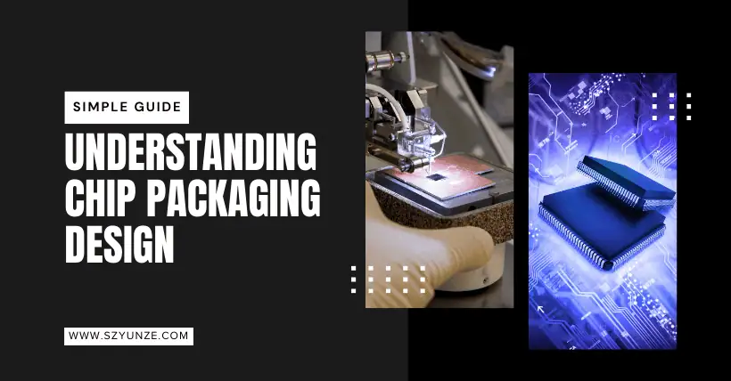
Packaging design is a crucial part of the integrated circuit (IC) manufacturing process, determining the functionality, reliability, and manufacturability of the chip.
1. Overall Objectives of Packaging Design
The primary goal of packaging design is to provide mechanical protection, electrical connections, and thermal management for the chip, ensuring stable operation during use. Through packaging, the chip establishes electrical and mechanical connections with external systems while ensuring effective heat dissipation.
Analogously, packaging acts as the “shell” and “support structure” of the chip, protecting it from environmental damage and facilitating information exchange with external devices.
2. Chip Layout and Die Placement Design
Chip layout is one of the core tasks in packaging design. The arrangement of chips is closely related to the package size, chip quantity, and dimensions. Common layout methods include:
- Planar Layout: Suitable for cases where the chip area is small and requires a large packaging space. All chips are arranged side by side on the same plane.
- Stacked Layout: Used when multiple large chips are involved, stacking them vertically to optimize space utilization and avoid excessive proximity between chips or between the chips and the package edge.
- Hybrid Layout: A combination of planar and stacked arrangements, balancing space utilization and manufacturability, commonly seen in high-integration System-in-Package (SiP) designs.
For example, in SiP designs, chips with different functions need to be allocated strategically to balance functional integration and heat dissipation.
3. Component Placement and Integration Density
When component density is high in IC design, the spacing between components becomes crucial. Smaller spacing improves system integration and functionality density but must also ensure manufacturability. For example, multiple passive components and dies can be arranged optimally to maintain high integration while preventing interference.
This process is similar to organizing furniture and objects in a compact space—each item must serve its function while maintaining adequate spacing to avoid unnecessary conflicts or issues.
4. Wire Bonding Design
Wire bonding is a classic chip interconnection technology widely used in various packaging types. It connects wires to the chip’s bonding pads, transmitting electrical signals to external circuits. As packaging complexity increases, wire bonding design also becomes more challenging.
- Selecting the appropriate wire type and diameter: Depending on chip size, power requirements, and package type, different wire materials (such as gold or aluminum) and diameters are chosen to ensure good electrical performance and thermal conductivity.
- Connection method design: Proper wire layout at different chip positions, such as handling corner bends and stacking chip connections, prevents excessive bending that may lead to instability.
This is similar to wiring an electrical device—ensuring appropriate wire length, thickness, and bending angles to prevent poor current flow or circuit failures.
5. Flip-Chip (FC) Technology
Flip-chip (FC) technology differs from traditional wire bonding by flipping the chip so that its electrodes make direct contact with the pads on the substrate, enabling electrical connections. FC technology offers several advantages:
- Better electrical performance: Reduces wire resistance and parasitic capacitance, improving signal transmission speed and current-carrying capacity.
- Smaller package size: Without the need for wire bonding space, FC packaging is more compact, meeting high-density integration demands.
- Enhanced thermal management: FC technology facilitates rapid heat transfer, improving cooling efficiency and preventing overheating.
Flip-chip technology can be likened to assembling a puzzle upside down, where pieces connect directly to the base, eliminating extra connection steps, making the process more streamlined and efficient.
6. Packaging Design and System-Level Optimization
Packaging design is not only about individual chip connections and heat dissipation but also about addressing overall system requirements. For example, in SiP designs, multiple chips and components with different functions are integrated into a single package. Designers must consider electrical performance, mechanical strength, and thermal management to ensure system stability and reliability.
This is similar to assembling a multifunctional electronic device—each component has a specific role, and optimizing their integration within a limited space is key to achieving the best performance.
Conclusion
Packaging design is a critical step in IC manufacturing, directly impacting electrical performance, heat dissipation, mechanical strength, and manufacturability. From chip layout and wire bonding to flip-chip technology, every design detail affects the final product’s stability and performance. As integration demands grow more complex, packaging design must consider multiple factors to ensure products meet all performance requirements.

Disclaimer:
- This channel does not make any representations or warranties regarding the availability, accuracy, timeliness, effectiveness, or completeness of any information posted. It hereby disclaims any liability or consequences arising from the use of the information.
- This channel is non-commercial and non-profit. The re-posted content does not signify endorsement of its views or responsibility for its authenticity. It does not intend to constitute any other guidance. This channel is not liable for any inaccuracies or errors in the re-posted or published information, directly or indirectly.
- Some data, materials, text, images, etc., used in this channel are sourced from the internet, and all reposts are duly credited to their sources. If you discover any work that infringes on your intellectual property rights or personal legal interests, please contact us, and we will promptly modify or remove it.