
Traditional data storage has always relied on switching between “on” and “off” states, but the physical size of the components that store these binary states limits the amount of information that can be contained in a device.
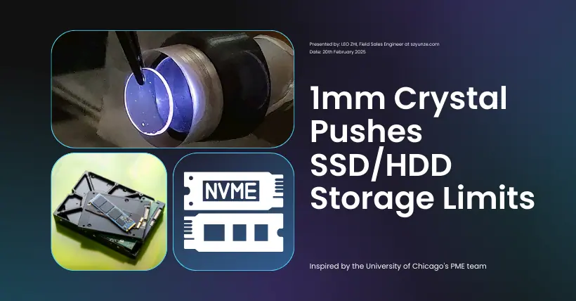
Recently, researchers from the University of Chicago’s PME team published their findings, showing that they successfully stored several terabytes of data within a crystal just 1 millimeter in size, marking a groundbreaking milestone for future storage solutions.
According to reports, the researchers achieved this goal by using single-atom defects within the crystal to represent binary 1s and 0s for data storage.
The study, published in the journal Nanophotonics, explores how atomic-scale crystal defects can serve as individual storage units and how quantum methods can be integrated with traditional computing principles.
The researchers believe that this breakthrough could redefine the limits of data storage, providing super-light, super-high-capacity storage solutions for traditional computing.
The first author of the study, postdoctoral researcher Leonardo Fran?a, said: “We have found a way to combine solid-state physics applied to radiation dosage measurement with research teams focusing on the quantum field.”
Under the leadership of Assistant Professor Tian Zhong, the research team developed this innovative storage method by introducing rare-earth ions into the crystal, specifically doping praseodymium ions into yttrium oxide crystals. They believe that due to the diverse optical properties of rare-earth elements, this method could be extended to other materials.
The memory system is activated by ultraviolet lasers that can energize the rare-earth ions to release electrons, which are then trapped in natural defects within the crystal.
By controlling the charge states of these defects, the researchers effectively created a binary system, where charged defects represent 1s and uncharged defects represent 0s.
In the past, crystal defects had been explored as potential quantum bits (qubits) in quantum computing research. Now, the University of Chicago’s PME team has further discovered how to apply these defects in traditional storage applications.
Sourcing from Internet
Related:
- How Rare Earth Materials Influence Chip Development
- How Concentration Polarization Affects Wafer Quality?
- Deep Dive into Hot Spot Tech in Chip Failure Study
- NVIDIA Unveils Silicon Photonics Switch with TSMC Tech
- Understanding Intrinsic Semiconductors and Its Behavior

Disclaimer:
- This channel does not make any representations or warranties regarding the availability, accuracy, timeliness, effectiveness, or completeness of any information posted. It hereby disclaims any liability or consequences arising from the use of the information.
- This channel is non-commercial and non-profit. The re-posted content does not signify endorsement of its views or responsibility for its authenticity. It does not intend to constitute any other guidance. This channel is not liable for any inaccuracies or errors in the re-posted or published information, directly or indirectly.
- Some data, materials, text, images, etc., used in this channel are sourced from the internet, and all reposts are duly credited to their sources. If you discover any work that infringes on your intellectual property rights or personal legal interests, please contact us, and we will promptly modify or remove it.